Metasurfaces have attracted great attention due to their ability to manipulate the phase, amplitude, and polarization of light in a compact form. Tunable metasurfaces have been investigated recently through the integration with mechanically moving components and electrically tunable elements. Two interesting applications, in particular, are to vary the focal point of metalenses and to switch between holographic images. We present the recent progress on tunable metasurfaces focused on metalenses and metaholograms, including the basic working principles, advantages, and disadvantages of each working mechanism. We classify the tunable stimuli based on the light source and electrical bias, as well as others such as thermal and mechanical modulation. We conclude by summarizing the recent progress of metalenses and metaholograms, and providing our perspectives for the further development of tunable metasurfaces.
Metasurfaces are composed of two-dimensional (2D) periodic arrays of subwavelength-scale artificial elements, called meta-atoms. They have attracted great attention due to their ability to manipulate the properties of electromagnetic waves.1–8 Several design methods have been proposed with various shapes and compositions of meta-atoms.8,9 The Pancharatnam–Berry (PB) phase, also called geometric phase, has been investigated using rectangular-shaped meta-atoms that impart a phase delay proportional to their rotation angle. Propagation phase has been investigated by exploiting an effective refractive index to manipulate the retardation phase by changing the volume ratio, aspect ratio, and height of meta-atoms.10,11 Resonant effects such as plasmonic resonance,12–15 Mie resonance,16,17 and Fabry–Pérot resonance18,19 have also been exploited. By exploiting these resources, optical elements can be highly miniaturized and various optical applications have been implemented, such as beam splitters,20–22 absorbers,23–29 metalenses,30,31 metaholograms,32–40 selective thermal emitters,41–43 detecting devices,44–46 and structural color.47–52
The functionality and efficiency of metasurfaces have been continuously increased by improving the methods to design meta-atoms, and the development of their material composition. Achromatic metalenses have been fabricated using complex geometric-structured meta-atoms that have a wide phase-dispersion set, and therefore enable achromatic focusing with single-layered metasurfaces.53 Furthermore, complex-amplitude metaholograms have been proposed by varying the conversion efficiency of meta-atoms to enable three-dimensional (3D) images.54,55 In terms of the materials, the use of resin with embedded nanoparticles30,31,56 has been proposed as a method to achieve mass production of dielectric metasurfaces through single-step direct nanoimprinting. Low-loss hydrogenated amorphous silicon57 has been proposed for low-cost deposition of visibly transparent thinfilms, and the fabrication cost is much lower and its modulation efficiency is compatible with that of titanium dioxide ()58 and gallium nitride (GaN)59,60 metasurfaces that work at visible frequencies.
Tunable metasurfaces with multiple functionalities through the active control of electromagnetic waves have been actively studied.61,62 Tunable metasurfaces are made up of meta-atoms that are controlled by external stimuli such as electrical biases or high-intensity light sources. Electrical, thermal, and mechanical stimuli have been used to induce two or more optical responses in single- or double-layered metasurfaces. Also, manipulation of the polarization state of the incident light that changes the output wavefront has been used to provide tunable functionalities for metasurfaces. Tunable metasurfaces provide multiple functionalities, however, generally have limitations in that the efficiency is generally worse than conventional passive metasurfaces, due to inherent problems such as the properties of tunable materials and design principles.1,3,9,63,64
Sign up for Advanced Photonics TOC. Get the latest issue of Advanced Photonics delivered right to you!Sign up now
In this review, we define “tunable metasurface” as one that can induce two or more optical responses due to variations in the incident light, or to changes to the meta-atom configuration or relative distances between two adjacent metasurfaces. Additionally, we present recent advances in tunable metasurfaces, in particular, tunable metalenses and metaholograms. Tunable metalenses and metaholograms are important applications of tunable metasurfaces. In the case of tunable metalenses, there is an advantage that it can be applied to an ultrathin zoom lens that can replace bulky optical components required for conventional optical devices.61,65 Meanwhile, owing to the high capacity of tunable metaholograms, it is expected to be one of the fundamental technologies of future metasurface integrated devices, such as holographic memory devices and ultrahigh-density display applications.54,66,67 However, once the fabrication is undertaken, it is difficult to change the period and size of the meta-atoms. In addition, complete modulation principles capable of nanoscale local pixel control have not been established.
In this review, we first briefly introduce the fundamentals of metalenses and metaholograms. Most tunable optical responses are obtained by controlling the light source or through an applied voltage, so we classify tuning methods as (1) controlling the light source, (2) electrical tuning, and (3) non-electrical tuning. Non-electrical tuning includes heat-induced phase change materials (PCMs), mechanical deformation, and changes of a relative position of cascaded metasurfaces. Finally, we summarize the overall contents, and suggest future directions of research on tunable metasurfaces.
2 Tunable Metalenses
2.1 Design Principles of Metalenses
Conventional refractive and diffractive lenses have a tradeoff relationship between miniaturization and optical characteristics.68 For example, to achieve achromatic focusing, several diffractive or refractive lenses must be used, but it can be achieved using single-layer metasurfaces.60 To design metalenses, the desired phase profile should be physically constructed using meta-atoms. To focus an incident plane wave at a lens focal point, the target phase at a point on a metalens should satisfy the phase retardation.9where is the radial distance from the center to each point, is the focal length, and is the wavelength. The distance between the focal point and a point on a metasurface varies with so as to correct for the distance difference, and the meta-atoms should satisfy the phase retardation [Eq. (1)] to achieve constructive interference at the focal point. To design tunable metalenses, meta-atoms must have properties that can change their optical responses so that they satisfy Eq. (1).
To achieve tunable metalenses, some mechanisms such as helicity or spin sensitive geometric phase, liquid crystals (LCs) or graphene-integrated lenses, and PCMs or stretching methods have been used. Active materials such as LCs or graphene can be integrated with metalenses to modulate the phase profile for achieving focus tuning. Their electrically controllable characteristics such as different alignment (LC) and Fermi level and carrier density (graphene) can be used, depending on the external electric field. Moreover, modulating refractive index using PCMs can be used in achieving tunable metalenses. Finally, a method of changing the geometrical parameters of the metalens through stretching flexible substrates can be used.
2.2 Tunable Metalenses by Light Source
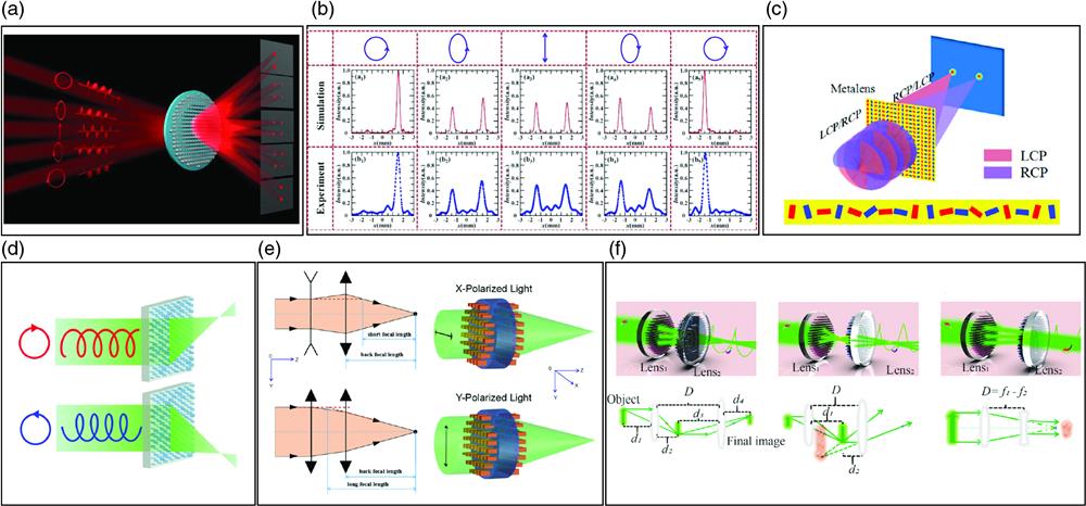
Tunable metalenses can be realized to control properties of light sources such as the polarization state. Spin-decoupled metalenses have been achieved using PB phase to integrate the properties of multiple convex and concave lenses into one metasurface:69 one phase profile focuses left-circularly polarized (LCP) incident light, while the other profile focuses right-circularly polarized (RCP) light. Therefore, the focal point changes when the polarization of incident light changes [Fig. 1(a)]. Additionally, the intensity of multiple focal points can be tuned by controlling the ellipticity of incident light [Fig. 1(b)]. Using only the geometric phase, it has the simplicity of designing a spin decoupled metalens instead of using both the propagation phase and geometric phase because of no need for scanning lots of parameters. However, the proposed metalens has a low efficiency of in theory.
Figure 1.Tunable metalenses by light source. (a) Schematic illustration of spin-decoupled metalenses.69 (b) Simulated and experimental electric field intensity distributions at line for multiple polarization states of incident light (LCP, LECP, LP, RECP, RCP from left to right).69 (c) Schematic of spin selective metalenses that can focus RCP and LCP incident beams to different focal points.70 (d) Schematic view of metalenses using the combination of the PB phase and propagation phase.71 (e) Schematic of step-zoom metalenses in which the focal length is changed according to the linear polarization of the incident light.72 (f) Schematic of metalenses doublet that has different functions depending on the polarization of the incident light.73
Multiple focal points can be generated by controlling the circular polarization state of incident light. Helicity-dependent multifocal metalenses can create multiple focal points in different directions when the polarization of the incident light changes.74 These metalenses are composed of anisotropic rods that have different orientations and can be considered as half waveplates with a high efficiency. Its polarization-conversion efficiency is at 0.64 THz under LCP illumination.
Furthermore, a spin-selected metalens that has a 0.98 numerical aperture (NA) value (simulated data) can focus incident light at two focal points depending on the spin state of the incident light.70 It is composed of a unit structure of silicon nanobricks, and the desired phase profile is implemented by the PB phase. Two silicon nanobricks (red and blue) on the metalens act as a convex lens or a concave lens when the spin state of the incident light changes [Fig. 1(c)]. This spin-selected metalens is useful for applying detecting techniques and spin controlled photonics.
The focal point can be adjusted by combining the PB phase and the propagation phase.71,75 One spin-multiplexed metalens uses the PB phase and propagation phase of nanorods.71 It makes a polarization-independent hyperbolic phase and a polarization-dependent linear phase, depending on the polarization state of the incident light, and therefore has different focal points for LCP and RCP light [Fig. 1(d)]. The diameter and NA of this lens are 1.8 and 0.05 mm, respectively. Although the NA is low, this lens demonstrated diffraction-limited focusing. Furthermore, is used to obtain high modulation efficiencies in the visible band by exploiting its low loss extinction coefficient and high refractive index. This metalens has an advantage of high focusing efficiency (maximum of 70%). But it is more complex for designing a metalens; it is a tradeoff relationship between efficiency and designing simplicity.
A step zoom metalens that has dual focal lengths and 0.21 NA value has been demonstrated using double-sided metasurfaces.72 These metasurfaces are composed of an array of silicon nanobricks, and the desired phase is obtained by changing the lengths of their long and short axes. Under polarized light, the first metasurface operates as a concave lens, and the second one operates as a convex lens. In contrast, under -polarized light, both metasurfaces operate as convex lenses [Fig. 1(e)]. Consequently, focal lengths vary depending on the linear polarization state of incident light. This double-sided metasurfaces design technique has advantages such as compactness, simplicity, and flexibility; and it has great potential for applications in biomedical sciences, optical communications, and wearable electronics.
Additionally, a metalens doublet that has different functions depending on the polarization of the incident light and the distance between two lenses has been reported.73 The first 0.258 NA metalens is composed of nanocylinders with different diameters to implement the propagation phase. It is therefore polarization-independent. The second metalens has an NA of 0.66 and is composed of rectangular meta-atoms to implement the PB phase, making it a polarization-dependent lens. The two lenses are used in tandem to implement a three-function lens doublet by varying the circular polarization state of the incident light and the distance between the lenses [Fig. 1(f)]. This metalens doublet has the advantages of making the imaging system simple and compact because no additional optical components are required for the multifunctional system. Therefore, it has great promising perspectives for applications in portable imaging systems.
2.3 Tunable Metalenses by Electrical Bias
Electrically tunable metalenses can be realized by applying an external voltage bias on active materials, such as LCs76–82 and graphene.83–89 Transmission-type terahertz metalenses that combine dielectric metasurfaces with photopatterned LCs have achieved tunable chromatic aberration.78 When the voltage bias is applied to the LCs, their geometric phase modulation vanishes, and only the resonant phase in the metalenses remains, so the function of the device changes from achromatic to dispersive focusing [Fig. 2(a)]. By integrating two functions into one metalens, it has great promising perspectives for applications in spectroscopy and imaging systems.
Figure 2.Tunable metalenses by electrical bias. (a) Schematic view of LC integrated metalenses that change functionality achromatic focusing to dispersive focusing when applying voltage bias to LCs.78 (b) Side view of TN LCs integrated electrically tunable metalenses. It modulates the polarization state of the incident beam depending on the applied voltage bias.79 (c) Schematic of a focus tunable graphene metalens when DC voltage bias is applied to this metalens.85 (d) Variation of focal length and focal spot intensity when the design is a packed pattern (top) and shifted bezel pattern (bottom).85 (e) Schematic of tunable graphene metalenses in which the chemical potential of graphene is controlled by applying a gate voltage.88 (f) Schematic view of electrically tunable metalenses in which the refractive index of BTO antennas is changed by applying voltage bias.90
A varifocal metalens that switches between NA 0.21 and 0.7 (simulated data) has been obtained by putting twisted nematic (TN) LCs under a metalens substrate.79 Depending on the voltage applied to the electrode, the TN LCs convert the polarization state of the incident light, and achieve different focal points for different polarization states of incident light [Fig. 2(b)]. Using the combination of a metalens and TN LCs, it has advantages of high image quality and fast response time (sub-millisecond level). Therefore, it has great potential for applications in biomedical and optical technology.
Recently, graphene has been used to achieve tunability.83–89,91–95 A graphene-based ultrathin square subpixel lens whose focal length can be controlled by a voltage bias has been demonstrated85 [Fig. 2(c)]. By applying the external bias voltage to multilayer graphene, the Fermi level and carrier concentration according to the location in multilayer graphene are changed, resulting in the change of absorption and transmittance of graphene. These changes cause a width change of arc ribbon-shaped graphene, resulting in the modulation of a Fresnel zone plate topology. Therefore, the focal length of the lens is modulated up to 19.42% (from 190 to ) [Fig. 2(d)]. Furthermore, this ultrathin lens mechanism can be applied to multifunctional autostereoscopic areas such as 3D hologram displays and acoustic applications owing to the advantages of its subpixel scale structure.
Additionally, tunable terahertz metalenses composed of a graphene monolayer and gold (Au) film have been demonstrated.88 The application of a voltage to graphene changes its chemical potential and permittivity. This change shifts the transmittance and phase of the incident light, and yields a tunability of focal length of about [Fig. 2(e)]. This design concept can be applied to active terahertz devices for imaging. Changing the refractive index of nanopillars by applying a voltage is another way to tune the focal length.90 A metalens composed of indium tin oxide (ITO) as a transparent electrode, barium titanate (BTO) nanopillars, and a substrate has been proposed.90 The refractive index of BTO is proportional to the induced electric field, so by exploiting the electro-optic effect of the BTO crystals, a phase change can be achieved by controlling the external voltage [Fig. 2(f)]. The refractive index of a particular area on metalenses can be tuned by changing the refractive index of the nanopillars without controlling the entire metasurface. This metalens has advantages such as high-speed modulation, compactness, and flexibility.
2.4 Tunable Metalenses by Non-Electrical Input
In this section, we introduce metalenses that are tuned non-electrically through mechanical actuation and PCMs. First, metalenses that are tuned using mechanical actuation can be realized by stretching or rotating the substrate. For actuation by stretching the substrate, the meta-atoms are placed on a stretchable substrate such as polydimethylsiloxane. The physical locations and therefore the periodicity of the meta-atoms increase when a uniform strain is applied to the substrate. Therefore, stretching the substrate causes a change of the spatial phase profiles, which is used to vary the focal length [Fig. 3(a)].96,102–105 In Fig. 3(b), experimental results including a longitudinal beam profile and intensity distribution according to the stretch ratio and stretch ratio versus focal length graph are shown. According to these results, the focal length gradually increases as the stretch ratio increases.96 The target wavelength of this zoom lens is 632.8 nm, but can be altered by changing the geometry and materials of the meta-atoms.
Figure 3.Tunable metalenses by non-electrical input. (a) Schematic of metalenses that are tuned mechanically by stretching the substrate to tune the focal length.96 (b) Measured longitudinal beam profiles according to different stretch ratios (top), intensity distributions of transmitted cross polarized light with different stretch ratios (bottom left), measured and calculated stretch ratio-focal length graph (bottom right).96 (c) Schematic illustration of metalenses that are tuned mechanically by rotating the substrate (left) and phase distribution of one of two lenses (right).97 (d) Schematic view of a tunable metalenses system that consists of two cubic metasurfaces.98 (e) Schematic illustration of MEMS tunable metalenses in which the focal length is tuned by controlling the distance between two lenses.99 (f) Schematic illustration of varifocal metalenses in which the focal length is tuned by exploiting the phase change of GSST by furnace annealing.100 (g) Schematic of varifocal metalenses using phase-change material . The phase of is changed by controlling the temperature, and the change affects the focal length.101
Recently, to realize varifocal metalenses, graphene has been used to achieve a range of focal length tuning.106 Graphene has an advantage of being suitable for designing broadband devices due to its dispersionless characteristics over a broadband wavelength region from the ultraviolet to the terahertz regime due to its lack of a bandgap. The focal length of the graphene oxide metalenses can be adjusted by for a single wavelength (red, green, and blue light) by stretching the metalenses laterally. Furthermore, rotation of a metalenses doublet can tune its focal length.107–110 Mutual rotation of doublet metalenses has been shown to tune the focal length using Moiré metalenses that are axially asymmetric doublet lens97 [Fig. 3(c)]. The demonstrated metalens has an NA of 0.5 at a target wavelength of 900 nm. This mechanism has an advantage in terms of the wide tuning range of the focal length from negative to positive, compared to other mechanisms such as Alvarez lenses98,111 and micro-electromechanical systems (MEMS).99,112–114
Other mechanical actuation mechanisms such as Alvarez lenses and tunable metalenses that integrate MEMS systems have been demonstrated. Varifocal metalenses using the Alvarez lens design have been fabricated by integrating two cubic metasurfaces; one example in particular has a tunable focal length in connections when it is laterally actuated using a translation stage [Fig. 3(d)].98 This mechanism has a large tuning range due to the inverse proportionality between the focal length and displacement for Alvarez lenses, but it is unsuitable for portable lens platforms owing to use of micrometer translation stage to actuate the metasurfaces laterally. Another tunable metalens has been obtained using MEMS by combining two metasurfaces99; one on a glass substrate and is static (); the other on a movable membrane (); the two metasurfaces are linked by electrostatic actuation, and the focal length is modulated by controlling the distance between the two [Fig. 3(e)]. The NA value of object space and image space is 0.16 and 0.014, respectively. Using this mechanism, high-speed electrical focusing and scanning of the imaging distance was achieved.
Furthermore, PCMs have been widely used to make tunable metalenses, by varying the phase of the PCM through the application of external stimuli such as optical pulses,115 thermal heating,100 and electrical heating.101,116–119 A rewritable device that uses (GST) exploits modulation of the state of GST by an optical pulse.115 When a GST thin-film is stimulated by a femtosecond laser pulse, it causes partial state transition of GST and causes phase patterning. Active metasurfaces using a related optical PCM, (GSST) have been demonstrated to realize a highly varifocal metalens that operates at and has NAs of 0.45 (amorphous) and 0.35 (crystalline).100 The state of GSST can be converted by furnace annealing, and the focal length is tuned depending on the state of GSST [Fig. 3(f)]. This mechanism is simple and compact compared to other mechanical mechanisms due to the absence of moving parts. Moreover, GSST has no critical thickness to fully reversible switching, unlike GST, which has a critical thickness . However, the crystallization time of GSST is in the order of microseconds, which is slower than that of GST.
A thermally modulated varifocal metalens with NAs of 0.714 and 0.608 (simulated data) using has also been proposed [Fig. 3(g)].101 By controlling the temperature of , its phase can be converted. The refractive index of varies depending on its phase; this change causes the phase shift of incident light, and thereby achieves tunable focal length. The target wavelength of this metalens is 1310 nm, so using as meta-atoms, high focusing efficiency can be achieved due to low absorption of in the near-infrared region, unlike GST.
3 Tunable Metaholograms
3.1 Design Principle of Metaholograms
Holographic technologies have exploited the characteristics of light, such as amplitude, phase, and polarization, to record and reconstruct the interference patterns of targeted objects. Previous holographic technologies have utilized spatial light modulators (SLMs) to produce 3D images. However, the pixel pitch of SLMs is limited to the micrometer scale, which results in low resolution, small viewing angles, unpredicted high-order diffraction, and sampling problems.120 Therefore, metasurface holograms that have a pixel subwavelength scale have received great attention to overcome the shortcomings of conventional holograms.121,122
To design these metaholograms, there exist two main challenges. First, calculating the phase map is needed for attaining the desired light propagation, and second, obtaining the proper meta-atom design necessary to physically implement the desired phase shift range from 0 to . In calculating the overall phase map, employing the Fourier hologram is the most well-known method, and can be retrieved using techniques such as the Gerchberg–Saxton (GS) algorithm, which has demonstrated holograms with an efficiency over 80%.19,123–125 Then, the continuous phase map should be quantized to a discrete phased map to be utilized with the designed meta-atoms. Recently, a topologically protected full phase with a reflective plasmonic metasurface has also been reported.126 However, the current design processes have limitations in that they can only realize quantized phase maps instead of a continuous phase map from the above design methods. Establishing the reliable process that can realize continuous phase maps is a challenging problem.127
Metaholograms can control the phase, amplitude, and even polarization by exploiting light-matter interactions at the subwavelength scale. However, conventional metaholograms, once manufactured, are limited to a single function. Above all, tunable metaholographic technologies focus on storing as many holographic images as possible in a single metasurface by exploiting light source properties and active materials. In this section, we review the achievements of tunable metaholograms by controlling light sources (Sec. 3.2), and using active materials (Sec. 3.3).
3.2 Tunable Metaholograms by Light Source
The properties of light including the amplitude, phase, and polarization can be modulated using various optical components such as lenses, beam splitters, wave retarders, and polarizers. Metasurfaces can also be designed to respond differently to the properties of incident light. A single metasurface can produce tunable hologram images by controlling the properties of incident light sources that enter the metasurfaces. In this section, we discuss tunable metahologram research that considers regulating the polarization state,128–135 orbital angular momentum (OAM),54,136–139 and coding incident beam.67,140–142 Above these, other methods include modulating the wavelength or angle of the incident beam, which have also been used to realize tunable holographic images. One such metaholographic device composed of heterogeneous meta-atoms, operates at the visible (532 nm) and near-infrared (980 nm) wavelengths.36 Also, angle-multiplexed metaholograms composed of dielectric U-shaped meta-atoms have been used by adjusting the angle of incident light.143
3.2.1 Tunable metaholograms by polarization state
Metasurfaces consist of artificially tailored meta-atoms that can manipulate the polarization state of an interacting light beam. These meta-atoms can be used to create dynamic holographic images by changing the polarization states of light sources. Using these properties, helicity-multiplexed reflective metaholograms have been reported.129 One helicity-multiplexed metasurface composed of silver nanorods on a Si substrate can reconstruct switchable images for RCP and LCP at a wavelength of 633 nm [Fig. 4(a)]. Clear holographic images are also obtained at other visible wavelengths [Fig. 4(b)]. This approach suggests solutions to several main problems with polarization tunable metaholograms such as image quality, efficiency, and broadband bandwidth.
Figure 4.Tunable metaholograms by light source. (a) Schematic of tunable metaholograms that generate dual images that can be changed by the polarization state of an incident light beam. (b) Experimentally obtained holograms at incident wavelengths of 24 nm (left) and 475 nm (right).129 (c) Design principle of OAM multiplexing metaholograms and metahologram images with a planar wavefront (). (d) Reconstructed images using four different OAM beams with topological charges , , 1, and 2.137 (e) Illustration of a video metahologram using OAM. (f) It changes their images depending on the angular momentum of the incident light.54 (g) Schematic of the reprogrammable metaholograms with the modulated incident beam by SLM. (h) The recorded images with the characterized incident light (left), with uniform laser light (middle), and the incident laser beam itself (right).140
Further, polarization-sensitive color-tunable metasurface holograms have been demonstrated.130 The metasurfaces are composed of three kinds of Si meta-atoms and are developed using PB phase to modulate the wavefronts of a visible hologram. Chiral metaholographic technologies have been extended by the propagation phase and PB phase.128 These metasurfaces are designed to respond to arbitrary orthogonal polarization states. This approach improves on previous metaholograms, which only work under orthogonal linearly or circularly polarized light. Use of planar chiral elements extended metaholographic technologies to planar chirality.131 When illuminated with circularly polarized light, the reflective metasurfaces reconstructed dual images, while absorbing the opposite circularly polarized light. This research enables demonstrated various developments of tunable metasurfaces such as full-color display applications, polarization switchable devices, and spatial separation of polarization information channels beyond holographic imaging.
Despite the endeavors to overcome the limitations of polarization switchable metaholograms, conventional metaholograms generate only two images in response to two orthogonal polarization states. Vectorial holography is an innovative technique that exploits metasurfaces that consist of meta-pixels composed of two orthogonal meta-atoms that can respond to multiple polarization states.132 A broadband reflective vectorial metahologram operated at four polarization states. Vectorial hologram extended the degree of freedom of metaholograms, which can switch only two images.
Polarization multiplexing can extend the manipulation channels and augment encryption capability.133 Single-layer metasurfaces can realize multiple independent phase profiles, which can contain distinct information under illumination of different polarization states of light. Such metasurface holograms are actively used in optical encryption144 and applications such as polarization analyzers. An orthogonally polarized metasurface hologram that uses the PB phase can enable direct detection of polarization states in a one-time measurement.134 Although the polarization-analyzing metasurface has a low efficiency () at , it works well producing holographic images over a broad range of wavelengths. A proposed new encryption process uses different metaholograms as the keys of imaging encryption.135 The process uses dual-channel Malus metasurfaces to exploit high-quality images, which can generate a matrix during the encoding and decoding processes. Different channels of the metasurface can contain different matrix information to increase the number of keys available to encryption or anti-counterfeiting systems.
Although polarization multiplexed metaholograms have achieved storing multichannel information by adjusting the incident polarization states, it is difficult to react to subtle polarization states due to the sensitivity of meta-atoms.
3.2.2 Tunable metaholograms by orbital angular momentum
OAM is a fundamental property of light that can be controlled. OAM can be applied as a method to multiplex metahologram images. A vortex beam carrying OAM has a helical wavefront and a spiral phase profile expressed by , where is the topological charge number and is the azimuth angle in cylindrical coordinates. The topological charge number can be arbitrarily controlled, thus the OAM mode of a vortex beam has the advantage of having infinite degrees of freedom, theoretically.145
Multi-momentum transformation metasurfaces have been demonstrated using OAM and the linear momentum of incident light.136 OAM has also been implemented as an information carrier for metaholographic technology.137 The holographic image is sampled using a 2D Dirac function related to OAM modes to reconstruct an OAM selective hologram. These OAM metasurfaces have been designed with four images in the spatial frequency domain by combining different states of OAM. Four holographic images under light with different topological charges (, , 1, and 2) are reconstructed [Fig. 4(d)]. Using similar methods, video-holographic metasurfaces have been demonstrated [Fig. 4(e)].54 In addition, OAM video-holographic experimental images with different topological charges are reconstructed [Fig. 4(f)]. More than two hundred images can be stored by exploiting independent OAM channels. The above methods are expected to be utilized in ultrahigh-density video-holographic devices.
Another new method combines polarization control and OAM selectivity for metasurface holograms.138 Through this method, a single metasurface can reconstruct multiple holographic images; polarization selectivity is controlled using the property of birefringence, and OAM selectivity is modulated by changing the topological charge. OAM-encrypted metasurface holograms that depend on the polarization states have been introduced.139 They consist of two metasurfaces: one to generate multiple OAM beams, and another to generate an OAM-selective hologram, which can be applied to an encryption system.
OAM holograms are emerging technologies that can contain infinite information, theoretically. However, they cannot implement broadband selective metaholograms and ultrafast switching. These challenges could be solved through the combination with RGB selective rules and vortex microlasers.
3.2.3 Tunable metaholograms by coded incident beam
SLMs or dynamic micro-mirror devices (DMDs) have been traditionally used to create dynamic holographic displays, but these approaches have been limited due to their large pixel sizes, which cause sampling problems, small viewing angles, and multiple-order diffractions.146,147 However, SLM and DMD combined with metasurfaces have been used to greatly complicate the information of the incident light by small-pixel coding of the metasurfaces. This method can increase the complexity of metasurface hologram design.
SLMs have been used to produce reprogrammable metahologram encryption algorithms by manipulating the light sources.140 The correct metaholographic image is only reconstructed when the incident light is modulated to a predesigned wavefront by the SLM, whereas a misleading image is shown for undesigned incident light [Fig. 4(g)]. The experimental image set verifies that the phase matrix of incident light can operate in an optical holographic encryption system [Fig. 4(h)]. Dynamic 3D metasurface hologram can store 28-bit different holographic images, and dynamically reconstruct a holographic image with high frame rate in the visible range.67 The proposed metasurface uses DMD to exploit dynamic space coding of the incident structured laser beam and can display 228 different frames and achieve a high frame rate of up to 9523 frames per second. Code-division multiplexing (CDM) dynamic metasurface holograms have been developed using DMD to generate structural light as the incident beam.141 Birefringent metasurfaces adopt the CDM principle to produce 32 distinct holograms. A new method of secret sharing using cascaded metasurface holograms has been demonstrated.142 The process uses metasurface hologram images as encoding keys in place of an SLM or DMD. Light propagation by the cascaded metasurfaces optically reconstructs the secret images with high fidelity and builds up the phase shift of both holograms. Employing additional components such as SLM or DMD is an excellent means of complicating information through small pixel coding at the metasurface. However, due to inherent limitations of SLM and DMD, it requires a lot of optical components to combine metasurfaces. To overcome these fundamental limitations, realizing SLM with a tunable metasurface has been reported.148
3.3 Tunable Metaholograms by Active Material
Metaholograms can also be tuned using active materials. The tuning methods generally apply external stimuli to a metasurface composed of active materials. External stimuli can be classified as electrical or non-electrical stimuli. Therefore, this section presents electrically tunable149–155 and non-electrically tunable34,156–164 methods to tune metaholograms.
3.3.1 Tunable metaholograms by electrical bias
LCs, conductive oxides, and semiconductors that undergo dramatic changes in response to electricity have been used as electrical tuning methods. Among them, LCs are mainly applied to generate different holographic images. LCs can be easily switched between liquid and solid-crystal states by applying an electrical field. This phase transition of LC can generate great optical birefringence, which can be utilized in tunable metaholograms. LCs can assume nematic, smectic, and isotropic phases [Fig. 5(a)]. The nematic phase has a fixed orientation, the smectic phase has a fixed orientation in well-defined planes, and the isotropic phase has random orientations.62 Therefore, LCs can be used to control the local birefringence, which is used to reconstruct various holographic images by exerting external electric fields.
Figure 5.Tunable metaholograms by electrical bias. (a) Schematic of three major states of LC (nematic, smectic, isotropic). (b) Design and demonstration of electrically tunable dielectric metasurfaces that use LCs.149 (c) Working principle of the electrically controlled digital metasurface device (DMSD). (d) SEM image of the DMSD and experimental results by independent control of seven electrodes.150 (e) Schematic of the bifunctional vectorial metasurfaces with LC analyzer. (f) SEM image of fabricated metasurfaces, and metaholograms that can be tuned by applying different voltages [scale bars: (left) , (right) ].152
Electrically tunable transparent holographic displays have been achieved by integrating dielectric metasurfaces with LCs.149 The displays can be induced to show resonance shifts twice the size of their line width, by applying a voltage through the metasurface. A switchable metasurface display achieving 53% efficiency at [Fig. 5(b)] has been proven. An electrically controlled digital metasurface device (DMSD) has been developed for light-projection displays.150 The DMSD has unit pixels composed of an Au nanorod metasurface, LC, and an ITO-coated superstrate to exert electric fields in each cell [Fig. 5(c)]. To further broaden the potential of DMSD, it is used in a numeric display composed of seven electrically manipulated segments [Fig. 5(d)]. Multifunctional polarization-dependent metasurfaces can be integrated with electrically tunable LC in the visible region.151 The proposed metasurfaces could combine the polarization-control ability of metasurfaces with the birefringence properties of LC. These devices provide a pragmatic method for dynamic addressable metasurface applications such as laser imaging detecting and ranging.
Further, a proposed photonic security platform uses dynamic vectorial holographic images of pixelated bifunctional metasurfaces.152 In the white light, the proposed metasurfaces show structural color prints, whereas when laser illumination passes through the metasurfaces, the encoded tunable metaholograms are reconstructed [Fig. 5(e)]. The device shows a reflective QR-code image and transmissive vectorial holograms [Fig. 5(f)]. When the QR code is captured, decipher keys about proper voltage values are transferred and the receiver can decode the real key using the vectorial holographic image. A proposed new optical encryption method exploits an improved computer-generated holography (CGH) algorithm to generate holograms that have quantitative correlation.153 A nematic LC layer realizes the function of dynamic holographic display. One set of electrical modulation patterns acts as encryption keys, and the receiver decrypts the message using both cipher text and a table transferred holographically. Electrically tunable metaholographic technologies have also been studied. An electromagnetic reprogrammable hologram device exploits 1-bit coding of the diodes on the metasurfaces.154 Additionally, a conducting polymer and polyaniline can be used to electrochemically control a metaholographic device.155 The reported work has contributed to realizing practical LC-integrated metaholographic displays with encryption systems and data storage. However, controlling LCs locally with nano pixel units through partial voltages and combining them with the metasurface are still a challenging problem.
3.3.2 Tunable metaholograms by non-electrical input
Various metaholograms have been accomplished using thermal,156–159 chemical,155,160–162 and mechanical163,164 methods. Thermally sensitive materials, especially PCMs, such as germanium antimony telluride (GST) and vanadium dioxide (), have been exploited for efficient thermal tuning. By heating the material, the crystallization of GST which has nonvolatile properties can be achieved. Also, , which has volatile properties, can undergo an insulator—metal phase transition at a heating temperature of around 68°C. Plasmonic metadevices that have switchable spin–orbit interactions have been evaluated.156 Metasurfaces that enable the spin Hall effect, vortex beam generation, and hologram are obtained using GST. The response of the metasurface can be changed by a change of the phase of GST between amorphous (ON) and crystalline (OFF). A broadband active metahologram that could operate in dynamic holographic imaging has been achieved by exploiting the temperature-dependent properties of .157 A single metasurface is composed of two sets of resonators: the passive one is simple metallic C-shaped split-ring resonators (SRRs); the active one is integrated SRRs. This device could reconstruct different images in the terahertz range.
The capability of a GST metadevice has been increased using multiple-state switching of photonic angular momentum coupling.158 The proposed metasurfaces could convert spin angular momentum to an OAM beam, depending on three states of GST [Fig. 6(a)]. They can also encrypt optical information using various hologram images at different crystallization levels of GST under RCP and LCP illumination [Fig. 6(b)]. Hybrid-state engineering of GST may also have applications for optical encryption.159 The GST metasurfaces hologram could provide a novel technique that is only recognizable when amorphous and crystalline states coexist, a semi-crystalline state. More discussion about PCM metasurfaces is listed in the conclusion with electrically tunable PCM metasurfaces.165,166
Figure 6.Tunable metaholograms by non-electrical input. (a) Changing phase geometry (amorphous, semicrystalline, crystalline) that can construct SAM-OAM conversion by tuning the crystallization level of GST. (b) SEM images of fabricated metasurfaces and two different metaholographic images in response to three crystallization levels (top: RCP, bottom: LCP).158 (c) Schematic of the hydrogenating metasurfaces. (d) Four different holographic images during two hydrogenation and two dehydrogenation processes.160 (e) Illustration of the surface pressure-responsive designer LC; (f) experimental results before (left, LCP) and after (right, RCP) surface pressure by touch of finger.164 (g) Schematic of a gas sensor with LC-integrated metahologram. (h) The gas sensor changes optical images when hazardous gas is detected.34
Chemical tuning methods usually exploit hydrogenation of the metasurfaces. Hydrogenation and dehydrogenation process can transform from metallic to dielectric material properties, which can be utilized to implement dynamic metaholograms. This method has been used to create addressable dynamic metasurface holograms that can use chemical reactions to manipulate subwavelength pixels.160 A metallic metasurface composed of magnesium (Mg) nanorods transforms the dielectric metasurfaces as a result of hydrogenation of Mg [Fig. 6(c)]. The devices show four dynamic metasurface holograms during the hydrogenation and dehydrogenation process [Fig. 6(d)]. A reconfigurable metasurface hologram that reconstructs switchable images by exploiting a quantified phase relation of the Fidoc method has been studied.161 The functionality of metasurfaces that use Mg nanorods has been improved to combine the display and holograms.162 The dynamic dual-function metasurfaces can generate a colorful display under white light and reconstruct holographic images under coherent light at . However, chemical tunable metaholograms require long phase transition times. To overcome this limitation, a metallic polymer combining with electrical tuning method has been implemented.167
A stimulus-responsive, electric, thermal and mechanical, dynamic metahologram has been obtained using a designer LC.164 The LCs can be modulated by three different methods and operate as a switch that could change the holographic images in real-time [Fig. 6(e)]. LC-integrated metasurfaces could reconstruct different images when subjected to different surface pressures [Fig. 6(f)]. This concept was further investigated to realize gas sensors using LC-integrated metasurfaces [Fig. 6(g)].34 It attaches gas-reactive LC on metaholograms, and it changes optical images when gas is detected [Fig. 6(h)]. These studies will be helpful for future touching controllable metasurfaces. However, it is limited to applying the appropriate pressure, so optimizing the design process is necessary.
4 Conclusion
Metasurfaces can offer unique phenomena to control light by interacting with subwavelength meta-atoms. However, conventional metasurfaces are limited to single functionality, and this constraint impedes potential applications after fabrication. To overcome this limitation, tunable metasurfaces are being developed.62 Here, we have presented an overview of the recent advances in the design of tunable metasurfaces.
We introduced tuning methods such as controlling the light sources or electrical fields, and using active materials. Of these methods, electrical tuning of active materials has received great attention because of its versatility to be integrated with electronics. The use of LCs, semiconductors, and conductive oxides has revealed novel opportunities, but the design of metasurfaces that are tuned electrically is still in its infancy. Furthermore, nonvolatile PCMs such as GST and GSST are not easily reversed back to their amorphous state from a crystalline state. Conventional GST metasurfaces usually require a melt-quenching process with cooling rates . However, electrical tuning methods that use well-designed micrometer-scale heaters to change GST phase have been developed.165,166 This method has opened a new class of mixed-mode optoelectronic devices that use GST. Metasurfaces that use PCM with electrical control may give a fresh view to reprogrammable metadevices, such as optoelectrical neuromorphic devices and dynamic holograms.
Table 1 shows a summary of the work presented in this review, focusing on tunable metalenses and metaholograms. The main goals of metalenses are to obtain multiple focal spots, and some research has been conducted to change states of focusing and defocusing. On the other hand, metaholograms have been studied as ways to store multiple images by changing the properties of the incident light and nanostructures. More recently, visualized sensing and optical metaholographic encryption have gained attention. In addition, to realize metasurface holographic technology, the dynamic control of the holograms is essential. Even if new approaches for dynamic holographic displays are proposed using SLM or DMD, fully developed metasurface holographic video displays have not been realized yet. OAM holograms that use complex-amplitude metasurfaces capable of more than two hundred independent channels have been proposed. This result is achieved in momentum space by manipulating complex amplitudes of the light. Then holographic videos are successfully realized at different image planes. This method may provide a method to achieve a metasurface video display.
The development of a new design method or fabrication methods will expand the degrees of freedom of meta-atom design. Accordingly, we expect that alternative design methods such as inverse design and machine learning can assist researchers in designing metasurfaces that have the desired optical and electrical responses.23,168–178 Also, recently developed 3D manufacturing methods of plasmonic and dielectric metasurfaces will enhance the flexibility of possible designs.179–182 The development of deep learning will improve human intuition and imagination, and their design will be realized with advanced 3D manufacturing methods. These will provide effective strategies to design complete tunable metasurfaces.
Jaekyung Kim received his BS degree in mechanical engineering at Pohang University of Science and Technology (POSTECH), Republic of Korea (2021). He is currently an MS/PhD student under the guidance of Prof. Junsuk Rho at POSTECH. His research interests focus on nanofabrication and dielectric metasurfaces.
Junhwa Seong received his BS degree in mechanical engineering at POSTECH (2021). He is currently an MS/PhD student under the guidance of Prof. Junsuk Rho at POSTECH. His research interests focus on nanofabrication and dielectric metasurfaces.
Younghwan Yang received his BS degree in mechanical engineering from Ajou University, Republic of Korea (2018). He is currently an MS/PhD student under the guidance of Prof. Junsuk Rho at POSTECH. He is a recipient of the Hyundai Motor Chung Mong-Koo fellowship, and of the NRF doctoral candidate fellowship
Seong-Won Moon received his BS and MS degrees in electronics engineering at Kyungpook National University in 2020. He is currently a PhD student under the guidance of Prof. Junsuk Rho at POSTECH. His research interests focus on metasurfaces with orbital angular momentum.
Trevon Badloe received his MPhys (hons) degree from the University of Sheffield, United Kingdom, in 2012, with a year of study abroad at the National University of Singapore in 2010. After three years of teaching courses in English and classical mechanics as an assistant professor at Yeungjin University, Republic of Korea, he started working toward his PhD in mechanical engineering at POSTECH, Republic of Korea, in 2017. His interests include tunable metamaterials and metasurfaces, and machine learning for the design and optimization of nanophotonic applications.
Junsuk Rho is a Mu-Eun-Jae endowed chair professor with a joint appointment in the Department of Mechanical Engineering and the Department of Chemical Engineering at POSTECH. He received his BS (2007) and MS (2008) degrees in mechanical engineering at Seoul National University and the University of Illinois, Urbana–Champaign, respectively. After getting his PhD (2013) in mechanical engineering and nanoscale science and engineering from University of California Berkeley, he worked as a postdoctoral fellow in the Materials Sciences Division at Lawrence Berkeley National Laboratory and as Ugo Fano fellow in the Nanoscience and Technology Division at Argonne National Laboratory.
[123] R. W. Gerchberg, W. O. Saxton. A practical algorithm for the determination of phase from image and diffraction plane pictures. Optik, 35, 237-249(1972).