• Advanced Photonics Nexus
  • Vol. 2, Issue 2, 026004 (2023)
Xiaowan Xu, Jiawei Wang, Yanjun Liu, and Dan Luo*
Author Affiliations
  • Southern University of Science and Technology, Department of Electrical & Electronic Engineering, Shenzhen, China
  • show less
    DOI: 10.1117/1.APN.2.2.026004 Cite this Article Set citation alerts
    Xiaowan Xu, Jiawei Wang, Yanjun Liu, Dan Luo. Large-scale single-crystal blue phase through holography lithography[J]. Advanced Photonics Nexus, 2023, 2(2): 026004 Copy Citation Text show less
    (a) BP I with body-center cubic lattice structure; (b) BP II with simple cubic lattice structure; (c) morphology of BP I(110) plane; (d) morphology of BP II(100) plane; (e) reduced morphology of BP I(110) plane; (f) reduced morphology of BP II(100) plane; (g) simplified grating of BP I(110) plane; (h) simplified grating of BP II(100) plane.
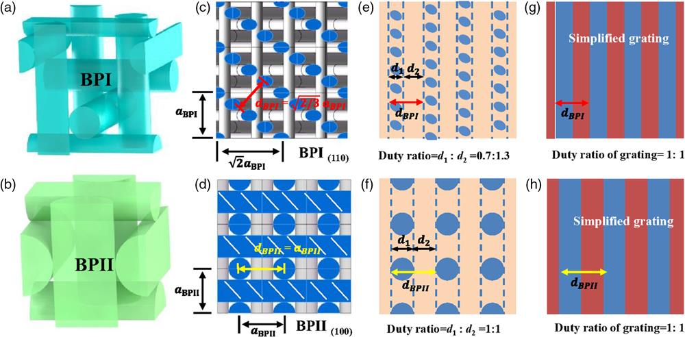
    Fig. 1. (a) BP I with body-center cubic lattice structure; (b) BP II with simple cubic lattice structure; (c) morphology of BP I(110) plane; (d) morphology of BP II(100) plane; (e) reduced morphology of BP I(110) plane; (f) reduced morphology of BP II(100) plane; (g) simplified grating of BP I(110) plane; (h) simplified grating of BP II(100) plane.
    Fabrication process of patterned substrate with periodic OTE grating for large-scale single-crystal BP generation. (a) Two-beam holography lithography based on the substrate with OTE and photoresist; (b) developing; (c) O2 plasma etching; (d) stripping; (e) periodic orientation of liquid crystal molecules induced by grating patterned substrate.
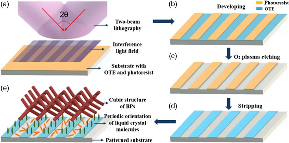
    Fig. 2. Fabrication process of patterned substrate with periodic OTE grating for large-scale single-crystal BP generation. (a) Two-beam holography lithography based on the substrate with OTE and photoresist; (b) developing; (c) O2 plasma etching; (d) stripping; (e) periodic orientation of liquid crystal molecules induced by grating patterned substrate.
    POM images of S1, S2, and S3 at different alignment conditions. S1 in BP I (a) at homeotropic alignment with polydomain, (b) at parallel alignment with monodomain, and (c) at grating alignment (d=230 nm) with single crystal. S2 in BP I (d) at homeotropic alignment with polydomain, (e) at parallel alignment with monodomain, and (f) at grating alignment (d=190 nm) with single crystal. S3 in BP II (g) at homeotropic alignment with polydomain, (h) at parallel alignment with monodomain, and (i) at grating alignment (d=170 nm) with single crystal. Scale bar: 100 μm.
    Fig. 3. POM images of S1, S2, and S3 at different alignment conditions. S1 in BP I (a) at homeotropic alignment with polydomain, (b) at parallel alignment with monodomain, and (c) at grating alignment (d=230  nm) with single crystal. S2 in BP I (d) at homeotropic alignment with polydomain, (e) at parallel alignment with monodomain, and (f) at grating alignment (d=190  nm) with single crystal. S3 in BP II (g) at homeotropic alignment with polydomain, (h) at parallel alignment with monodomain, and (i) at grating alignment (d=170  nm) with single crystal. Scale bar: 100  μm.
    Surface morphology of gratings, Kossel diagram, and reflection spectra of single crystals. SEM images of gratings were used to align of BP samples (a) S1, (b) S2, and (c) S3. The scale bar is 500 nm. (d) POM image of single crystalline BP I formed by S1. Inset: Kossel diagram of BP I(110); (e) POM image of single crystalline BP I formed by S2. Inset: Kossel diagram of BP I(110); (f) POM image of single crystalline BP II formed by S3. Inset: Kossel diagram of BP II(100). The reflection spectra of (g) S1, (h) S2, and (i) S3.
    Fig. 4. Surface morphology of gratings, Kossel diagram, and reflection spectra of single crystals. SEM images of gratings were used to align of BP samples (a) S1, (b) S2, and (c) S3. The scale bar is 500 nm. (d) POM image of single crystalline BP I formed by S1. Inset: Kossel diagram of BP I(110); (e) POM image of single crystalline BP I formed by S2. Inset: Kossel diagram of BP I(110); (f) POM image of single crystalline BP II formed by S3. Inset: Kossel diagram of BP II(100). The reflection spectra of (g) S1, (h) S2, and (i) S3.
    Photo images of (a) S1 in BP I, (b) S2 in BP I, and (c) S3 in BP II. Scale bar: 2 mm.
    Fig. 5. Photo images of (a) S1 in BP I, (b) S2 in BP I, and (c) S3 in BP II. Scale bar: 2 mm.
    SamplePhase TransitionTransition Temperature (°C)Pitch d (nm)Interference Angle θ (deg)Lattice Constant a (nm)Chiral Dopant Concentration c (wt.%)
    S1Iso-BP I89.223045.0281.73.0
    S2BP II-BP I85.819058.8232.73.6
    S3Iso-BP II88.517072.9170.03.4
    Table 1. Parameters of BP samples.
    SamplePitch d (nm)Calculated lattice constant a (nm)Measured lattice constant a (nm)Deviation value Δa (nm)
    S1231.5283.6289.35.7
    S2190.5233.3241.38.0
    S3170.9170.9161.69.3
    Table 2. Parameters of BP fabricated in our experiment.
    Xiaowan Xu, Jiawei Wang, Yanjun Liu, Dan Luo. Large-scale single-crystal blue phase through holography lithography[J]. Advanced Photonics Nexus, 2023, 2(2): 026004
    Download Citation