Abstract
The blue phase, which emerges between cholesteric and isotropic phases within a three-dimensional periodical superstructure, is of great significance in display and photonic applications. The crystalline orientation plays an important role in the macroscopic performance of the blue phase, where the single crystal shows higher uniformity over the polydomain and monodomain, resulting in higher Bragg reflection intensity, lower hysteresis, and lower driving voltage. However, currently reported methods of forming a single-crystal blue phase based on thermal controlling or e-beam lithography are quite time-consuming or expensive for large-scale fabrication, especially in the centimeter range, thus hindering the broad practical applications of single-crystal blue-phase-based photonic devices. Herein, a strategy to fabricate a large scale single crystalline blue-phase domain using holography lithography is proposed. Defect-free single-crystal domains both in blue phase I and blue phase II with a desired orientation of over 1 cm2 are fabricated based on a nanopatterned grating with periodic homeotropic and degenerate parallel anchoring, with colors from red and green to blue. This holography lithography-assisted strategy for fabrication of a large-scale single-crystal blue phase provides a time-saving and low-cost method for a defect-free single crystalline structure, leading to broad applications in liquid crystal displays, laser devices, adaptive optics elements, and electro-optical devices.1 Introduction
The blue phase (BP), existing between the cholesteric phase and isotropic phase (ISO) of liquid crystals within a three-dimensional periodical superstructure, possesses three forms of blue phase I (BP I), blue phase II (BP II), and blue phase III (BP III).1,2 BP III possesses a noncrystalline symmetry with disordered structure, and BP I and BP II exhibit body-centered cubic structure and simple cubic structure, respectively, with a double-twisted cylinder nanostructure.3–6 The narrowed temperature range and nonuniformity of the crystalline structure are two important issues that hinder the practical applications of blue phase liquid crystal (BPLC). On one hand, the temperature range of the BP has been extended by polymerization7,8 or nanoparticle doping,9,10 leading to useful applications such as displays,11–14 lasers,15–17 sensors,18–20 and photonic devices.21–24
On the other hand, the crystalline orientation plays an important role in the macroscopic performance of the blue phase, where the single crystal shows higher uniformity over the polydomain and monodomain, resulting in higher Bragg reflection intensity, lower hysteresis, and lower driving voltage. Usually, the BP fragments form inside the volume simultaneously as a phase transition occurs, leading to polydomain BP structures, which consist of many platelets of different orientations. The mismatches in polydomain BPs increase the scattering in the volume and affect the reflectivity of the Bragg reflection and the optical-electrical properties of BPs.25–29 Recent studies indicate that several methods, such as electric fields,30–32 thermal control,33 and surface treatments34–36 can be applied to form monodomain BPs, which consist of many single-crystal platelets with one lattice plane orientated in the same direction. The structures of monodomain BPs significantly increase the reflectivity of the Bragg reflection. However, many defects still exist between the separated platelets with a grain boundary. Therefore, to further improve the optical performance of BPs, it is highly desirable to develop methods of fabricating ideal, single-crystal BPs.
Several methods have been proposed to generate a single crystal blue phase. Chen et al.37 reported the fabrication of an extraordinarily large single-crystal BP I by controlling the self-assembly processes of BPLC. The gradient-temperature technique enables growth of a single crystalline BP with the size of . However, long periods of thermal control over several days were required, which leads to low efficiency in fabrication, and the crystal orientation of the BP could not be controlled due to the similar treatment of the substrate compared to traditional BPs. de Pablo et al. proposed a method to form a single crystalline BP II through a nanopatterned surface with binary homeotropic/planar anchoring through e-beam lithography.38–42 This method is capable of generating a single-crystal BP over a macroscopic region (at a scale of ) with designed crystallographic plane orientation based on the simulation of free energy from Landau–de Gennes theory (see Supplementary Material). However, the fabrication is highly dependent on the nanopattern fabricated by e-beam lithography, which is time-consuming and expensive, thus hindering the practical application of single-crystal BP photonic devices. Therefore, a time-saving and low-cost method, rather than e-beam lithography, to fabricate the nanopattern at a larger scale for large-scale single-crystal BPs is highly desirable.
Sign up for Advanced Photonics Nexus TOC. Get the latest issue of Advanced Photonics Nexus delivered right to you!Sign up now
In this paper, a strategy to fabricate large scale single crystalline BP liquid crystals is demonstrated through holography lithography. Defect-free single-crystal domains both in BP I and BP II with a desired orientation of over are fabricated based on a nanopatterned grating with periodic homeotropic and degenerate parallel anchoring. A large-scale single-crystal BP with reflection colors from red and green to blue are realized while varying the pitch of the nanopattern grating from 230 and 190 nm to 170 nm, along with a high reflectance of 44% and 45% to 42% and a narrow bandwidth of 19.0 and 17.0 nm to 14.6 nm, respectively. This holography lithography-assisted strategy for fabrication of a large-scale single-crystal BP provides a time-saving and low-cost method for a defect-free single-crystalline structure that significantly improves the property of the BP, including an increase in the intensity of the Bragg reflection, leading to broad applications such as liquid crystal displays, laser devices, adaptive optics elements, and electro-optical devices.
2 Results and Discussion
In our experiments, both BP I [with body-center cubic lattice structure, Fig. 1(a)] and BP II (with simple cubic lattice structure, Fig. 1(b)] are investigated. The wavelength of reflected light from the BP is determined by , where is the wavelength of reflective light, is the refractive index (; and are the ordinary and extraordinary refractive indices of liquid crystal materials), is the lattice constant of crystal, and are the Miller indices.1 The BP crystallographic planes are denoted by (), and represents a BP with orientation of the () plane parallel to the surface.

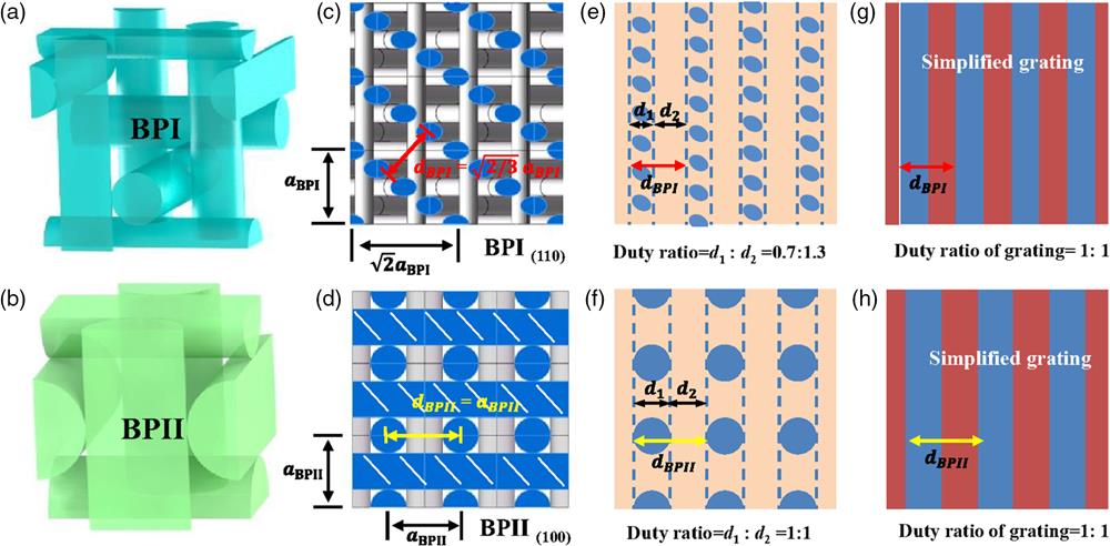
Figure 1.(a) BP I with body-center cubic lattice structure; (b) BP II with simple cubic lattice structure; (c) morphology of BP plane; (d) morphology of BP plane; (e) reduced morphology of BP plane; (f) reduced morphology of BP plane; (g) simplified grating of BP plane; (h) simplified grating of BP plane.
The anchoring pattern of the substrate is designed based on the morphology of the orientating lattice plane on the surface. Figure 1(c) shows the morphology of BP plane at the boundary of crystal lattice with (where means the displacement from the boundary of the unit lattice). The region of blue ellipses represents the cross section of a double-twist cylinder on the substrate surface, where the liquid crystal (LC) molecules orient from 45 deg to 90 deg (the angles between the substrate surface and the director of the LC molecule). This region will be treated to be a homotropic surface anchored in a simplified alignment model. The rest of the region represents the defect structure in the crystal lattice, which can be seen as isotropic materials. The pitch along two orthogonal directions is represented by , and , where is the lattice constant of BP I, leading to an effective period of grating formed by the region of blue ellipses to be . This region will be treated as a degenerate parallel surface anchored in a simplified alignment model. Figure 1(d) shows the morphology of BP , which is similar to BP I. The region of the blue rectangle with an oblique line represents the long-axis cutting section of the double-twist cylinder, where the LC molecules orient from 0 deg to 45 deg (the angles between the substrate surface and the director of LC molecule). Both the blue rectangle and the rest of the region will be treated as a degenerate parallel surface anchored in a simplified alignment model. The effective period of grating formed by the region of blue circles and the rest is .
The single crystalline BPs are mediated by the strain induced by the corresponding patterned anchoring conditions with the lower free energy. The grating pattern consists of homeotropic anchoring and degenerate parallel anchoring, resulting from boundary molecular distribution, which successfully induced the formation of single crystalline BPs.38,39
Figures 1(e) and 1(f) demonstrate the reduced morphology of BP and BP planes at the boundary of the crystal lattice with , where the blue region represents the homeotropic surface anchoring and the rest, the yellow region, represents degenerate parallel surface anchoring. The reduced morphology of surface anchoring can be further simplified to a grating in both cases, and the duty ratio is defined as , where and are the corresponding widths of the region with the blue part and the region without the blue part, respectively. The duty ratios are around 0.7:1.3 (where ) and 1:1 (where ) in Figs. 1(e) and 1(f), respectively. The morphologies under other cutting conditions are shown in Fig. S1 in the Supplementary Material ( to ) and Fig. S2 in the Supplementary Material ( to ), respectively. However, the fabrication process of the duty ratio (0.7:1.3) is much more difficult. Therefore, we try to use a grating with a duty ratio of 1:1 to replace the duty ratio of 0.7:1.3, which shows good and acceptable results in the following experiments. Figures 1(g) and 1(h) demonstrate the simplified grating deduced from Figs. 1(e) and 1(f), respectively. To reduce the difficulty of fabrication, the duty ratio of grating is chosen to be 1:1 in both cases. This simplification process proved to be effective and efficient, leading to a single crystal forming in both the BP and BP planes.
In our experiment, two-beam holography lithography was applied to generate the grating on a large scale. Figure 2(a) depicts the schematic illustration of the fabrication process, where a linearly polarized laser beam (the polarization direction is perpendicular to the plane of the optical table) with a wavelength of 325 nm splits into two beams by passing through a beam splitter, and there is interference at the surface of substrate coated with homeotropic alignment material (OTE) and photoresist. For two-beam holography lithography, the obtained interference light field is a grating. The pitch of the formed grating is determined by the formula of , where is the pitch of the grating, is the wavelength of the laser, and the interference angle is half the angle between two interference beams.
Figure 2.Fabrication process of patterned substrate with periodic OTE grating for large-scale single-crystal BP generation. (a) Two-beam holography lithography based on the substrate with OTE and photoresist; (b) developing; (c) plasma etching; (d) stripping; (e) periodic orientation of liquid crystal molecules induced by grating patterned substrate.
The parameters of BP samples (S1, S2, and S3) used in our experiment are shown in Table 1. The data indicate the process of phase transitions and the corresponding information between substrates and lattice parameters; for example, Iso-BP I means this sample is started from an isotropic phase and stabilized at BP I through cooling. Once the pitch is fixed, the corresponding interference angle, lattice constant, and chiral dopant concentration can be calculated. In our experiments, three pitches of grating were chosen to be 230, 190, and 170 nm, and the calculated interference angle should be 45.0 deg, 58.8 deg, and 72.9 deg, respectively. The corresponding lattice constant is calculated to be 281.7 and 232.7 nm for BP I (according to ), and 170 nm for BP II (according to ), which require the concentration of chiral dopant of R5011 () to be 3.0, 3.6, and 3.4 wt.%, respectively.
| Sample | Phase Transition | Transition Temperature (°C) | Pitch (nm) | Interference Angle (deg) | Lattice Constant (nm) | Chiral Dopant Concentration (wt.%) |
| S1 | Iso-BP I | 89.2 | 230 | 45.0 | 281.7 | 3.0 |
| S2 | BP II-BP I | 85.8 | 190 | 58.8 | 232.7 | 3.6 |
| S3 | Iso-BP II | 88.5 | 170 | 72.9 | 170.0 | 3.4 |
Table 1. Parameters of BP samples.
The pattern of the grating received by the positive photoresist where the bright region in the light field forming the grating will be developed and removed, while the dark region in the light field forming the grating will be retained for the next developing step [Fig. 2(b)]. After developing, the plasma etching was applied [Fig. 2(c)], where the OTE covered with photoresist (yellow) was kept from etching by plasma and while the OTE part uncovered with photoresist was etched. After stripping of the photoresist, a grating consisting of the region with OTE (which would lead to perpendicular alignment of the LC) and the region without OTE (which would lead to degenerate parallel alignment of the LC) on substrate were fabricated, as shown in Fig. 2(d). Figure 2(e) shows the orientation of liquid crystal molecules induced by the surface anchoring of the patterned substrate. The patterned homeotropic and degenerate parallel anchoring of the substrate induces periodic orientation of liquid crystal molecules on the patterned substrate and leads to uniform formation of BPs with a cubic structure. The cell with a grating pattern was made up of a bare glass and a glass with grating-patterned OTE, and spacers were used to define the cell thickness.
The phase transitions among isotropic phase, BP I, and BP II can be categorized as isotropic phase BP I, BP II–BP I, and isotropic phase BP II during the temperature decrease process. Figures 3(a)–3(c) show the polarization optical microscopy (POM) images of sample S1 in BP I (cooling from isotropic phase at 89.5°C to BP I at 85.7°C with a rate of 0.1°C/min) at the homeotropic, parallel, or grating-patterned alignment of the substrate, leading to polydomain, monodomain, and a single crystal, respectively. Figures 3(d)–3(f) show the POM images of sample S2 in BP I (cooling from isotropic phase at 88.8°C to BP II at 86.3°C and then to BP I at 84.9°C with rate of 0.1°C/min) at homeotropic, parallel, or grating-patterned alignment of the substrate, leading to polydomain, monodomain, and a single crystal, respectively. Figures 3(g)–3(i) show the POM images of sample S3 in BP II (cooling from isotropic phase at 89°C to BP II at 86.8°C with rate of 0.1°C/min) at homeotropic, parallel, or grating-patterned alignment of the substrate, leading to polydomain, monodomain, and a single crystal, respectively. The changes of the clear point and temperature range of BPs with these three surface treatments are negligible. The parallel anchoring derives from rubbing on polymide (PI) materials with one preferred azimuth in the horizontal direction, as shown in Figs. 3(b), 3(e), and 3(h). The uniformity of images from the homeotropic and parallel alignment-induced polydomain and monodomain BP are apparently worse than that from the grating alignment-induced single crystal. Polydomain BPs [Figs. 3(a), 3(d), and 3(g)] contain plenty of single crystals with different orientations and a disordered mosaic image with several colors. Monodomain BPs [Figs. 3(b), 3(e), and 3(h)] contain pieces of a single crystal with a uniform orientation but still with defects and inconspicuous boundaries between the pieces. In contrast, the patterned grating alignment successfully induces the single crystal [Figs. 3(c), 3(f), and 3(i)] in all three cases of S1, S2, and S3, where the pitch of grating is 230, 190, and 170 nm with corresponding reflection colors of red, green, and blue. The single crystal forms a uniform crystalline structure in a large domain of macroscopic size, and the obtained single crystal has no defect in the volume.
Figure 3.POM images of S1, S2, and S3 at different alignment conditions. S1 in BP I (a) at homeotropic alignment with polydomain, (b) at parallel alignment with monodomain, and (c) at grating alignment () with single crystal. S2 in BP I (d) at homeotropic alignment with polydomain, (e) at parallel alignment with monodomain, and (f) at grating alignment () with single crystal. S3 in BP II (g) at homeotropic alignment with polydomain, (h) at parallel alignment with monodomain, and (i) at grating alignment () with single crystal. Scale bar: .
Figures 4(a)–4(c) demonstrate the images of fabricated three gratings observed under scanning electron microscopy (SEM). The experimentally measured pitch is 231.5, 190.5, and 170.9 nm, respectively, which is highly consistent with the designed pitch of , , and . The POM images of S1, S2, and S3 (corresponding to grating patterned in Figs. 4(a)–4(c), respectively) with corresponding Kossel diagrams (as inset figures) for the lattice planes of BP , BP , and BP are shown in Figs. 4(d)–4(f), respectively. According to the principle of lattice diffraction,3 the Kossel diagrams of BP have six lines in Fig. 4(d) and four lines in Fig. 4(e), which derives from diffractive limitation. The lattice constant of sample S1 is larger than S2 within diffractive limitation; therefore, more Kossel lines can be seen. The Kossel diagrams with distinct Kossel lines indicate a uniform orientation. The Bragg reflection spectra of S1, S2, and S3 are shown in Figs. 4(g)–4(i), respectively. The single-crystal BPs of samples S1, S2, and S3 possess high reflectance of 44%, 45%, and 42% (the theory limitation is 50% due to the circularly polarized light of reflection) at central wavelengths of 648, 540, and 512 nm, and narrow bandwidths of 19.0, 17.0, and 14.6 nm, respectively. According to the relationship of the grating period and the lattice constant for BP I and BP II (, and ), the calculated lattice constants of induced single-crystal BPs are , , and , respectively. Compared to the measured lattice constants () of 289.3, 241.3, and 161.6 nm, the deviation values between the calculated and measured values of lattice constants are 5.7, 8.0, and 9.3 nm, respectively, which are quite small compared to those previously reported in Ref. 38. The parameters including pitch, calculated and measured lattices, and the deviation values for samples S1–S3 are shown in Table 2.
Figure 4.Surface morphology of gratings, Kossel diagram, and reflection spectra of single crystals. SEM images of gratings were used to align of BP samples (a) S1, (b) S2, and (c) S3. The scale bar is 500 nm. (d) POM image of single crystalline BP I formed by S1. Inset: Kossel diagram of BP ; (e) POM image of single crystalline BP I formed by S2. Inset: Kossel diagram of BP ; (f) POM image of single crystalline BP II formed by S3. Inset: Kossel diagram of BP . The reflection spectra of (g) S1, (h) S2, and (i) S3.
| Sample | Pitch (nm) | Calculated lattice constant (nm) | Measured lattice constant (nm) | Deviation value (nm) |
| S1 | 231.5 | 283.6 | 289.3 | 5.7 |
| S2 | 190.5 | 233.3 | 241.3 | 8.0 |
| S3 | 170.9 | 170.9 | 161.6 | 9.3 |
Table 2. Parameters of BP fabricated in our experiment.
The reflection spectra and POM textures of BPs are valid proof to differentiate polydomain, monodomain, and single-crystal BPs, as shown in Fig. S3 in the Supplementary Material. The polydomain BPs are easy to differentiate. The spectra of monodomain and single-crystal BPs are quite similar, which makes them difficult to distinguish. Monodomain BPs are formed with pieces of single crystals with the same orientationand show similar Bragg structure colors. The defects and mismatches of angles between pieces of crystalline structures exist in monodomain BPs, while single-crystal BPs exhibit perfect morphology in the POM texture.
Figures 5(a)–5(c) show the photo images of fabricated single-crystal BPs S1, S2, and S3 with a large scale of over in red, green, and blue, respectively. In principle, the fabrication size can be further increased by using a larger diameter of laser beam with higher laser power. The large scale of single-crystal BPs based on holography lithography induced grating pattern of the substrate enables defect-free crystalline structures, leading to potential applications in displays, lasers, and electro-optical devices.
Figure 5.Photo images of (a) S1 in BP I, (b) S2 in BP I, and (c) S3 in BP II. Scale bar: 2 mm.
3 Conclusion
We demonstrated a strategy to fabricate a large-scale single crystalline BP through holography lithography. Defect-free single crystals both in BP I and BP II with size over are fabricated based on a nanopatterned grating with periodic homeotropic and degenerate parallel anchoring. The grating pattern consisting of homeotropic anchoring and degenerate parallel anchoring resulting from boundary molecular distribution successfully induced the formation of a single crystalline blue phase. A single-crystal BP in BP , BP , and BP planes with reflection color from red and green to blue are realized while varying the pitch of the nanopattern grating from 230 and 190 nm to 170 nm, with a high reflectance of 44% and 45% to 42% at the central wavelengths of 648 and 540 to 512 nm, and narrow bandwidths of 19.0 and 17.0 nm to 14.6 nm, respectively. This holography lithography-assisted strategy for fabrication of a large-scale single-crystal BP provides a time-saving and low-cost method for formation of a defect-free single crystalline structure, leading to broad applications in liquid crystal displays, laser devices, adaptive optics elements, and electro-optical devices.
4 Experimental Section
4.1 Materials
Liquid crystal host HTG135200-100 (, of 589 nm at 20°C) and chiral dopant R5011 () were purchased from Hecheng Display. Homeotropic alignment materials octadecyltriethoxysilane [OTE, ] were purchased from Sigma Aldrich and used without further purification. Parallel alignment material polyimide (PI) was purchased from Beijing Bomi Company. Photoresist mr-P 1202LIL, developer mr-D 374 and stripper mr-Rem 660 (based on N-methylpyrrolidon (NMP)) were purchased from Micro Resist Technology.
4.2 Fabrication Process
Liquid crystal mixtures preparation: The nematic liquid crystal HTG135200-100 and chiral dopant R5011 were mixed together, stirred at the isotropic phase, and cooled down to the BP.
Substrates preparation: First, the OTE film was developed on the substrates. The substrate glass was cleaned by sonication in acetone and ethyl alcohol. The glass was immersed in the mixture of concentrated and 30% aqueous (2:1 v/v) for 30 min. The samples were immersed in the mixture of 240 mg OTE and 70 ml toluene with 0.25 mL as catalyst for 90 min. The samples should be vertically inserted into the solution and should not touch each other. To remove excess silane aggregates in the solution, the samples were stirred in a toluene bath and rinsed with deionized water several times. Then they were blown dry with nitrogen and allowed to cure for 2 h at 150°C in a vacuum oven. After development with OTE, the substrates were spin-coated with photoresist mr-P 1202LIL (4000 r, 30 s) and baked at 100°C for 60 s, and then exposed under two-beam interference for 30 s to get the structure of the grating. A 325 nm He–Cd laser was used as the interference light source. The substrate was developed in developer mr-D 374 for 25 s. The resulting grating pattern was transformed onto the OTE film layer by exposing the sample to oxygen plasma (50 W, 60 s), followed by stripping the photoresist in stripper mr-Rem 660 for 1 min.
The cell with the grating pattern was made up of a bare glass and a glass with grating-patterned OTE, and spacers were used to define the cell thickness. A liquid crystal mixture was injected into the cell through capillary action. The cell was heated until the mixtures were at the isotropic phase, and then slowly cooled down by 0.1°C per minute until the single crystalline BP was fully formed in the cell.
The cell with homeotropic alignment was made up of a bare glass and a glass coated with OTE, which was an intermediate product in substrate preparation before photolithography.
The cell with parallel alignment was made up of a bare glass and a glass coated with PI. The PI-coated glass was rubbed with fabric beforehand to induce parallel alignment.
4.3 Measurements
Optical characterization was performed by using the cross-polarized and reflective mode of the microscope (ECLIPSE Ci POL, Nikon) with a objective. Samples were heated up and cooled down by using a temperature controller hot stage (TS62, INSTEC). Visible spectra of BPs were obtained by spectrometer (USB2000+, Ocean Optics). The He–Cd laser (IK3151R-E, KIMMON) was used to generate two-beam interference. The laser power was 10 mW, and the beam diameter of laser beam was 2 cm.
Xiaowan Xu received her PhD from the Department of Electrical and Electronic Engineering, Southern University of Science and Technology. She currently works at Shenyang Ligong University. Her research interests include blue phase liquid crystal devices, single crystalline blue phases, and nanofabrication.
Jiawei Wang is currently a PhD candidate in the Department of Electrical and Electronic Engineering, Southern University of Science and Technology. His research interests include optical metasurfaces and their dynamic modulation, liquid crystal photonic devices, and nanofabrication.
Yanjun Liu received his PhD in photonics from Nanyang Technological University, Singapore, in 2007. He is currently an associate professor in the Department of Electrical and Electronic Engineering, Southern University of Science and Technology, China. His research group mainly focuses on liquid crystal photonics, active plasmonics, and metamaterials/metasurfaces. He has authored/co-authored more than 200 peer-reviewed journal publications, 10 granted patents, 5 book chapters, and 30 invited talks in his research fields.
Dan Luo received his PhD in photonics from Nanyang Technological University, Singapore, in 2012. He is currently an associate professor in the Department of Electrical and Electronic Engineering, Southern University of Science and Technology. His research interests include liquid crystal photonic devices, liquid crystal optical sensor, and liquid crystal elastomer actuator. He has published more than 140 peer-reviewed journal publications with citation of more than 2600 times and H-index of 27.
References
[1] D. C. Wright, N. D. Mermin. Crystalline liquids: the blue phases. Rev. Mod. Phys., 61, 385-432(1983).
[2] W. Hu et al. Ultrastable liquid crystalline blue phase from molecular synergistic self-assembly. Nat. Commun., 12, 1440(2021).
[3] S. Meiboom, M. Sammon, W. F. Brinkman. Lattice of disclinations: the structure of the blue phases of cholesteric liquid crystals. Phys. Rev. A, 27, 438-454(1983).
[4] S. S. Gandhi, L.-C. Chien. Unraveling the mystery of the blue fog: structure, properties, and applications of amorphous blue phase III. Adv. Mater., 29, 1704296(2017).
[5] H. M. Jin et al. Soft crystal martensites: an in situ resonant soft x-ray scattering study of a liquid crystal martensitic transformation. Sci. Adv., 6, 5986(2020).
[6] J. Liu et al. Diffusionless transformation of soft cubic superstructure from amorphous to simple cubic and body-centered cubic phases. Nat. Commun., 12, 3477(2021).
[7] H. Kikuchi et al. Polymer-stabilized liquid crystal blue phases. Nat. Mater., 1, 64-68(2002).
[8] D. M. Xu et al. Electro-optic response of polymer-stabilized blue phase liquid crystals. Appl. Phys. Lett., 105, 011119(2014).
[9] H. Yoshida et al. Nanoparticle-stabilized cholesteric blue phases. Appl. Phys. Express, 2, 121501(2009).
[10] M. Ravnik et al. Three-dimensional colloidal crystals in liquid crystalline blue phases. Proc. Natl. Acad. Sci. U. S. A., 108, 5188-5192(2011).
[11] F. Castles et al. Stretchable liquid-crystal blue-phase gels. Nat. Mater., 13, 817-821(2014).
[12] Y.-S. Zhang et al. Stretchable freestanding films of 3D nanocrystalline blue phase elastomer and their tunable applications. Adv. Opt. Mater., 9, 2001427(2020).
[13] F. Meng et al. High-resolution erasable “live” patterns based on controllable ink diffusion on the 3D blue-phase liquid crystal networks. Adv. Funct. Mater., 32, 2110985(2022).
[14] Y. Huang et al. Optimized blue-phase liquid crystal for field sequential-color displays. Opt. Mater. Express, 7, 641-650(2017).
[15] M. Wang et al. Bias-polarity dependent bidirectional modulation of photonic bandgap in a nanoengineered 3D blue phase polymer scaffold for tunable laser application. Adv. Opt. Mater., 6, 1800409(2018).
[16] G. Petriashvili, A. Chanishvili. Liquid crystal blue phases interconversions based real-time thermal imaging device. Opt. Express, 27, 13526-13531(2019).
[17] J. Liu et al. Single-, dual-, triple-, and quadruple-wavelength surface-emitting lasing in blue-phase liquid crystal. Adv. Mater., 34, 2108330(2022).
[18] V. Sridurai et al. Electrically tunable soft photonic gel formed by blue phase liquid crystal for switchable color-reflecting mirror. ACS Appl. Mater. Interfaces, 9, 39569-39575(2017).
[19] Y. Yang et al. Structural and optical response of polymer-stabilized blue phase liquid crystal films to volatile organic compounds. ACS Appl. Mater. Interfaces, 12, 42099-42108(2020).
[20] Y. Yang et al. Bioinspired color-changing photonic polymer coatings based on three-dimensional blue phase liquid crystal networks. ACS Appl. Mater. Interfaces, 13, 41102-41111(2021).
[21] F. Castles et al. Blue-phase templated fabrication of three-dimensional nanostructures for photonic applications. Nat. Mater., 11, 599-603(2012).
[22] J. Yang et al. Photonic shape memory polymer based on liquid crystalline blue phase films. ACS Appl. Mater. Interfaces, 11, 46124-46131(2019).
[23] W. Hu et al. Humidity-responsive blue phase liquid-crystalline film with reconfigurable and tailored visual signals. Adv. Funct. Mater., 30, 2004610(2020).
[24] K. R. Schlafmann, T. J. White. Retention and deformation of the blue phases in liquid crystalline elastomers. Nat. Commun., 12, 4916(2021).
[25] R. Manda et al. Polymer-stabilized monodomain blue phase diffraction grating. Adv. Mater. Interfaces, 7, 1901923(2020).
[26] E. Oton et al. Orientation control of ideal blue phase photonic crystals. Sci. Rep., 10, 10148(2020).
[27] E. Oton et al. Monodomain blue phase liquid crystal layers for phase modulation. Sci. Rep., 7, 44575(2017).
[28] K. Kim et al. A well-aligned simple cubic blue phase for a liquid crystal laser. J. Mater. Chem. C, 3, 5383-5388(2015).
[29] P. Nayek et al. Effect of the grain size on hysteresis of liquid-crystalline Blue Phase I. J. Soc. Inf. Disp., 20, 318-325(2012).
[30] Y. Chen, S.-T. Wu. Electric field-induced monodomain blue phase liquid crystals. Appl. Phys. Lett., 102, 171110(2013).
[31] M. Chen et al. Electrically assisting crystal growth of blue phase liquid crystals. Opt. Mater. Express, 4, 953-959(2014).
[32] J. Yan et al. A full-color reflective display using polymer-stabilized blue phase liquid crystal. Appl. Phys. Lett., 102, 081102(2013).
[33] H.-S. Chen et al. Hysteresis-free polymer-stabilized blue phase liquid crystals using thermal recycles. Opt. Mater. Express, 2, 1149-1155(2012).
[34] Z. G. Zheng et al. Light-patterned crystallographic direction of a self-organized 3D soft photonic crystal. Adv. Mater., 29, 1703165(2017).
[35] S. Liu, I. Nys, K. Neyts. Two-step photoalignment with high resolution for the alignment of blue phase liquid crystal. Adv. Opt. Mater., 10, 2200711(2022).
[36] J. Xiong et al. Holo-imprinting polarization optics with a reflective liquid crystal hologram template. Light Sci. Appl., 11, 54(2022).
[37] C. W. Chen et al. Large three-dimensional photonic crystals based on monocrystalline liquid crystal blue phases. Nat. Commun., 8, 727(2017).
[38] J. A. Martinez-Gonzalez et al. Directed self-assembly of liquid crystalline blue-phases into ideal single-crystals. Nat. Commun., 8, 15854(2017).
[39] X. Li et al. Perfection in nucleation and growth of blue-phase single crystals: small free-energy required to self-assemble at specific lattice orientation. ACS Appl. Mater. Interfaces, 11, 9487-9495(2019).
[40] X. Li et al. Mesoscale martensitic transformation in single crystals of topological defects. Proc. Natl. Acad. Sci. U. S. A., 114, 10011-10016(2017).
[41] X. Li et al. Sculpted grain boundaries in soft crystals. Sci. Adv., 5, 9112(2019).
[42] X. Li et al. Nucleation and growth of blue phase liquid crystals on chemically-patterned surfaces: a surface anchoring assisted blue phase correlation length. Mol. Syst. Des. Eng., 6, 534-544(2021).