Abstract
A suspended dual- microstrip meander-line (SDMML) slow wave structure (SWS) was proposed. It consists of a metal enclosure as well as a suspended dielectric substrate, on the upper and lower surfaces of which are two metal meander-lines. As there are two electron beam tunnels locating above and below the dielectric substrate, and the electromagnetic wave has symmetrical distribution, it is possible to use one electron beam in each tunnel to drive the electromagnetic wave for a higher output power. The high frequency characteristics and the beam-wave interaction results of the SDMML SWS have been investigated by using simulation software. The hot performances of this SWS show that for two identical sheet beams with a voltage of 2050 V and a current of 0.2 A, the SDMML SWS has a maximum gain of 26 dB at 36 GHz and 3-dB bandwidth of saturation power of 8 GHz. To verify the simulation result, a SDMML SWS is fabricated by using new fabrication methods including the magnetron sputtering electroplate and laser ablation. The measured reflection loss of the SDMML SWS is better than -10 dB. The transmission loss of the fabricated slow wave structure is analyzed and verified through simulation and experimental results.Introduction
With the development of various applications,higher frequency,lower operating voltage,higher output power and miniaturization have been the requirements for TWTs [1]. In recent years,the planar SWSs which were proposed to reduce the size and facilitate fabrication have obvious advantages in packaging volume. As a kind of typical planar SWS,the microstrip meander-line SWSs have attracted a growing interest [2-5]. The more important,they are compatible with modern microfabrication technologies and capable of adopting a high-current,high-aspect-ratio sheet electron beam. Such microstrip meander-line SWSs were supposed to provide high slow-wave factor for low operating voltage,for example,the operating voltage of these planar microstrip SWS could be 3∼10 kV at millimeter-wave band [6-9]. As the application scenarios increase,the lower operating voltage SWSs have greater advantages.
Generally,lower operating voltage means lower overall input power,and if the interaction efficiency is not improved,the output power of the SWS will also be reduced. Increasing the input power or interaction efficiency by taking certain measures is an effective method to increase the output power. One solution widely employed by researchers for improving interaction efficiency is using symmetrical meander-line SWSs [9-11]. By placing two SWSs symmetrically above and below the electron beam channel,the electric field distribution is changed to improve the coupling impedance of the SWS,so,the interaction efficiency is increased. Another solution is designing some planar SWSs that can interact with the two sheet-beams [12-14]. Using two sheet-beams can increase the input power without increasing the current density.
In this paper,we proposed a SDMML SWS,which consists of two SDMMLs on the top and bottom surfaces of the suspended dielectric substrate. A metal enclosure is then employed to hold the suspended substrate. The odd mode with smoother dispersion characteristics is adopted as the operation mode,of which the operating voltage will decrease to 2 kV. By taking advantage of the double slow-wave structure with dual sheet electron beams,the input power can be increased and a larger output power can be achieved within the relatively short tube length. In order to meet the requirements of the vacuum devices,new fabrication method is tried,including magnetron sputtering,electroplate and laser ablation. The SDMML SWS is achieved with a metal layer of sufficient thickness to resist bombardment of electrons. We have completed the cold testing on the SDMML SWS. The cold testing results were analyzed and the improved fabrication method is provided.
This paper is organized as follows. The structure and dimension parameters of the SDMML SWS are described in Sect. 1,as well as the high frequency characteristics. The beam-wave interaction results are given in Sect. 2. The results of transmission characteristics are demonstrated. For verifying transmission characteristics of the SWS,the fabrication process and cold testing of that is outlined in Sect. 3. In the last,some useful conclusion is present in Sect. 4.
1 The high frequency analysis of the SDMML SWS
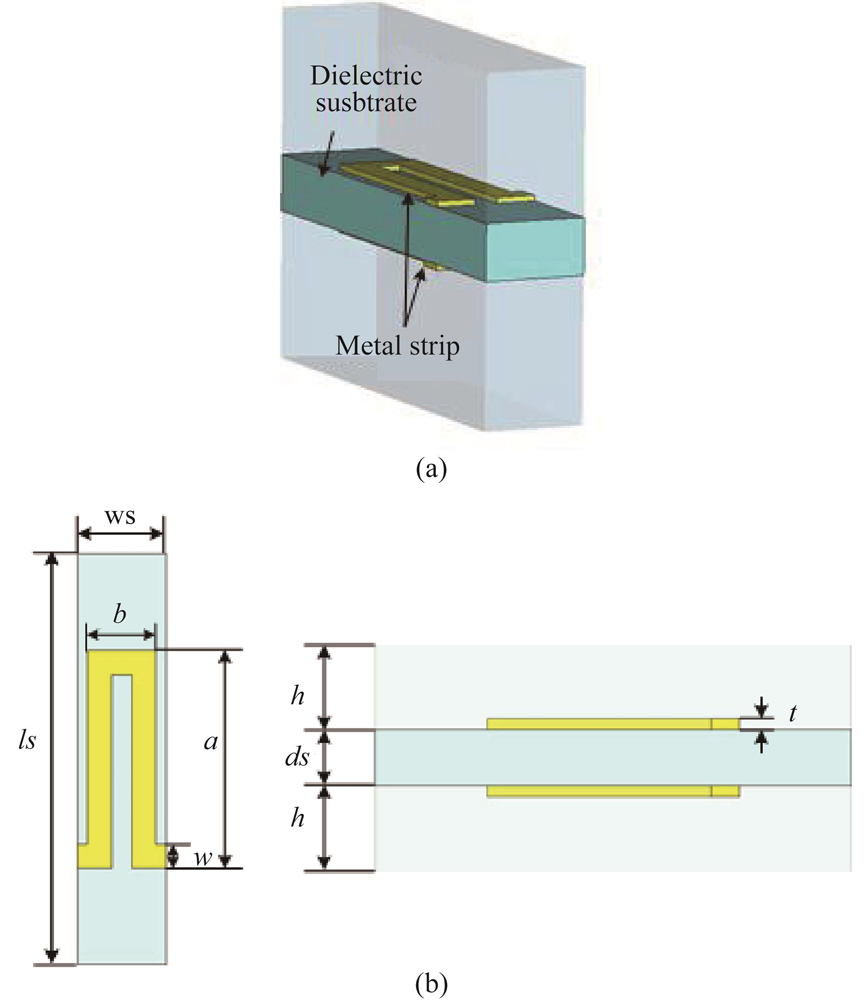
The unit periodic model of the SDMML SWS is illustrated in Fig. 1. As can be seen,there are two metal meander-line strip placed on the top and bottom surfaces of the suspended dielectric substrate. In order to ensure that the upper and lower tunnels have symmetrical electric field distribution,the optimal suspension position of the SWS should be at the center of the tunnel in the height direction,so that the top and bottom tunnels are completely symmetrical. The advantages of the suspended dielectric substrate include decreasing the phase velocity of the electromagnetic wave and increasing the interaction impedances of SWS. The detailed structural parameters are listed in Table 1. Here,the metal meander line is set to copper with a thickness of 0.01 mm and the substrate is set to alumina ceramic(εr = 9.9).
| Parameters | Value | Parameters | Value |
|---|
| a/mm | 0.8 | w/mm | 0.1 |
| b | 0.184 | h/mm | 0.5 |
| t/mm | 0.01 | ls/mm | 1.6 |
| ws/mm | 0.368 | ds/mm | 0.2 |
Table 1. Dimensional parameters of the designed SWS

Figure 1.(a)The diagram unit model of the SDMML SWS,and (b) size view
Due to the presence of a double layer of metal meander-line strip in the SWS,the entire structure constitutes a three-conductor transmission line system. In the transmission mode of the three-conductor system there are odd mode and even mode,the electric fields of which are shown in Fig. 2. Figure 3 shows the dispersion diagram of the odd and even modes of this SWS. The dispersion curve of odd mode is flattering and with a smaller slope than that of the even mode,which means that the odd mode will have broader bandwidth and lower operating voltage. According to the odd-mode dispersion curve in Fig. 3,the operating voltage of the structure at Ka-band is as low as 2 kV,which benefits from the usage of high dielectric constant alumina substrate and the optimization of the ratio between the transverse length and the period length of the SWS unit. Figure 4 shows the comparison of interaction impedance curves between the odd mode of this structure and the typical conventional microstrip SWS,which predicts that the SDMML SWS has higher interaction impedance than that of the conventional microstrip SWS.
Figure 2.The electric field of (a) the odd mode, and (b) the even mode
Figure 3.The dispersion curves of the SDMML SWS
Figure 4.The interaction impedance curves of the odd mode of the SDMML SWS and conventional microstrip SWS
2 The hot performance results of the SDMML SWS
Based on the analysis of the high-frequency characteristics of this SWS,we determined the specific operating parameters for the hot performance simulation,as shown in Table 2. In order to obtain the best hot performance results,two identical ideal sheet beams are assumed to flow 0.05 mm above the SWS. The beam voltage is 2050 V and the total current is 0.2 A(the current of single beam is 0.1A)throughout the simulation. A solenoidal magnetic field of 0.2 T is assumed to focus the sheet beams. Meanwhile,the copper conductivity are set to 5.96×10⁷ S/m and the dielectric constant and loss tangent of alumina ceramic is 9.9 and 0.0004,respectively. For an input power of 50 mW,the hot performance results including the output power and gain of the SDMML SWS with single beam and dual beam are shown in Fig. 5(a). The maximum output power is 20 W at 36 GHz,the corresponding gain and electronic efficiency being 26 dB and 5%. The 3-dB bandwidth is 4 GHz from 33 to 37 GHz. The saturation output power and gain are demonstrated in Fig. 5(b). Compared with the results of the same input power,the output power of the dual-beam case is about 3 dB higher that the single beam case,and the former’s 3-dB bandwidth of saturation power is wider from 32 GHz to 40 GHz.
Figure 5.(a) Output power, gain and (b) saturation power, gain curves of the SDMML SWSs with single and dual beam
| Operating parameters | Value | Operating parameters | Value |
|---|
| Voltage | 2050 V | Beam-SWS distance | 0.05 mm |
| Current | 0.1 A*2 | Focusing magnetic field | 0.2 T |
| Cathode size | 0.8 mm*0.2 mm | Input signal power | 50 mW |
Table 2. The operating parameters for hot performance simulation
Figure 6 shows the electron bunching phenomenon of the sheet beams above the SDMML SWS. The process of beam-wave exchange is demonstrated clearly by the phenomenon that the electrons are retarded and accelerated periodically. The output signal reaches a stable state and remains,after 2 ns simulation time. Fig. 7 shows the frequency spectrum(35 GHz)of the output port signal. The sharp spectrum peak indicates that the output signal is highly monochromatic.
Figure 6.Electron bunching above the SDMML SWS
Figure 7.Frequency spectrum of output signal(35 GHz)
3 Transmission characteristics simulation and test of the SDMML SWS
The transmission model of the SDMML SWS is established,as shown in Fig. 8,which consists of a section of 30-period SWS,two sections of tapered transition structures and a pair of input/output dual ridges waveguide couplers. The tapered transition structures located at both ends of the SWS are well designed to guarantee good transmission characteristics of the SWS. The dual ridges waveguide coupler is chosen to be the coupler of this SWS,because of its higher power capacity and mode transfer function. Using the dual ridges waveguides,we managed to convert the electromagnetic wave from a waveguide mode to an odd mode of the SDMML SWS. The waveguides are standard Ka-band rectangular waveguide with the cross-sectional dimension of 3.556 mm×7.112 mm. In the same way as the hot performance simulation,the materials of the meander -line and dielectric substrate used in the simulation models are copper and alumina,respectively. The electric conductivity of copper is set to 5.96×10⁷ S/m. The dielectric constant and the loss angle tangent of alumina are set to 9 .9 and 0.0004,respectively. The simulated S-parameters of the whole transmission model are shown in Fig. 9,in which the reflection loss(S11)can be read as less than -13 dB at the frequency range from 26 GHz to 40 GHz,while the transmission loss(S21)is greater than -7 dB. The loss is mainly caused by the conductor loss. Because the size of the metal line cross section is much smaller than that of waveguide,the conductor loss of metal line is larger.
Figure 8.The model of the SDMML SWS with the input/output coupler
Figure 9.The simulation transmission characteristics curves of the whole structure
The bonding strength between the metal layer and the dielectric substrate of conventional microstrip is low,and it will peel off after the vacuum high temperature treatment. Therefore,we design a new fabrication method for the SDMML SWS. To strengthen the bonding strength between the metal layer and dielectric substrate,magnetron sputtering and electroplating are used for the manufacturing of metal layers. First,we perform magnetron sputtering on the cleaned alumina ceramic surface. The metal layers of magnetron sputtering are divided into two layers,the first layer is titanium and the second layer is copper. Titanium as the active metal has a good bonding effect and can effectively bond the copper layer to the alumina ceramic firmly. The thickness of metal layers by magnetron sputtering is very small,usually less than 1 μm. The thicknesses of the titanium layer and copper layer are 500 nm and 1 μm,respectively. Then we use electroplating to thicken the copper layer up to 10 μm. After electroplating,the solidity and thickness of the metal layer can meet the requirements. The picosecond laser is utilized to burn out the shape of the meander line. Fig. 10 shows the meander line of the SDMML SWS. From the figure,it can be seen that the SWS have a complete shape and good machining accuracy between top and bottom faces.
Figure 10.The SDMML SWS after laser processing (a) top view, (b) bottom view.
Figure 11 shows the cold test model and fabricated model of the SDMML SWS. The cold test model includes the dual ridges waveguides and the SWS channel. The model is divided into two parts,which are symmetrical to each other and play a fixed clamping role for the SDMML SWS in the middle,as shown in Fig. 11(a). After assembly of the two parts,the cold test is carried out. The cold test results are obtained and shown in Fig. 12. The measured S11 is very similar with the simulated result and it is better than -10 dB in the frequency range of 30∼40 GHz. However,the measured S21 is about -20 dB in the frequency range of 30∼40 GHz. In Fig. 9,the simulation S21 is about –7 dB. It is clear that the measured insertion loss is much higher than the simulated loss.
Figure 11.The cold testing tube model and the pictures of the SDMML SWS and test tube
Figure 12.The cold testing result of the SDMML SWS
We subsequently investigated and confirmed the reasons for the unexpected high insertion loss. The first reason is attributed to the conductor loss of the meander line. The fabricated meander line consists of two layers:500 nm thick titanium and 10 μm thick copper. The conductivity of titanium,which is 2.38 × 10⁶ S/m,has not been considered in the original simulation. The second reason is the dielectric loss of the oxidation of the copper layer,which is caused by the heat of laser processing,as shown in Fig. 13. The copper oxide is a lossy material that has not been considered in the simulation.
Figure 13.(a) Diagram of oxidation area of the copper layer processed by laser, and (b) the model of oxidation area in simulation
Further simulations have been carried out to verify the reasons of high insertion loss,and the results are shown in Fig. 14. As can be seen,the titanium layer brought in 5 dB more insertion loss compared to pure copper layer. The thickness of the titanium layer is one twentieth of the thickness of the copper layer,but it has a relatively distinct effect in transmission losses [15]. At room temperature,copper oxide is a kind of dielectric material,and its dielectric constant and loss angle tangent are 18.1 and 0.1,respectively [16-18]. Applying copper oxide layer will cause serious dielectric loss,we investigated the effect of the copper oxide layer with thicknesses of 0.5 µm and 1 µm and found that at least 10 dB more insertion loss is observed. The insertion loss increases as the oxide layer thickness increases. By comparing the experimental loss and the modified simulation loss,it can be seen that the experimental loss is caused by the conductor loss of the titanium layer and the dielectric loss of the copper oxide as we analyzed.
Figure 14.The comparison of transmission loss S21 of experiment and some kind of simulated models
In view of the above discussion,there are two issues that need our attention in the subsequent processing. In order to reduce the transmission loss,on one hand,high-conductivity metals should be used instead of the low-conductivity metal layer as bonding layers. On the other hand,the metal layer should be protected by inert gases during the laser cutting process to prevent the generation of the oxidation area.
4 Conclusion
This paper has described the design,simulation,fabrication and cold testing the SDMML SWS at Ka-band. As a three-conductor transmission line structure,the SDMML SWS have odd and even modes. The odd mode has a lower operating voltage and wider bandwidth compared to the even mode. The suspension feature of this structure makes it suitable for double electron beam interactions and can effectively increase the electron beam input power. The operating voltage and current of this SWS are 2050 V and 0.2 A. From the particle-in-cell simulation,the maximum output power is 20 W at 36 GHz,corresponding gain and efficiency of 26 dB and 5%,respectively. The 3-dB bandwidth of saturation power is 8 GHz.
The transmission characteristics of the SDMML SWS have been studied and the cold test results have been analysis. The reflection loss(S11)of cold testing results has a good match with the ideal simulation results,which is below -10 dB from 30 to 40 GHz. But the transmission loss(S21)cannot match with the ideal simulation results. The low conductivity metal and some oxidation area have a serious impact on transmission loss. Therefore,the selection of a high conductivity metal as the bonding layer and the protection of the metal layer from oxidation should be focused in the processing of planar microstrip SWS.
References
[1] C K Chong, W L Menninger. Latest advancements in high-power millimeter-wave helix TWTs. IEEE Trans. Plasma Science, 38, 1227-1238(2010).
[2] H Booske2J, R J Dobbs, C D Joye et al. Vacuum electronic high power terahertz sources. IEEE Transactions on Terahertz Science and Technology, 1, 54-75(2011).
[3] F Shen, Y Y Wei, H R Yin et al. A novel V-shaped microstrip meander-line slow-wave structure for W-band MMPM. IEEE Trans. Plasma Science, 40, 463-469(2012).
[4] N M Ryskin, A G Rozhnev, A V Starodubov et al. Planar microstrip slow-wave structure for low-voltage V-band traveling-wave tube with a sheet electron beam. IEEE Electron Device Letters, 39, 757-760(2018).
[5] A I Benedik, A G Rozhnev, N M Ryskin et al. Planar V-band slow-wave structures for low-voltage tubes with sheet electron beam, 1-2(2017).
[6] S M Wang, Y B Gong, Y Hou et al. Study of a log-periodic slow wave structure for Ka-band radial sheet beam traveling wave tube. IEEE Trans. Plasma Sci., 41, 2277-2282(2013).
[7] A V Starodubov, V V Galushka, R A Torgashov et al. Planar slow-wave structures for low-voltage millimeter-band vacuum devices (Novel approach for fabrication, numerical and experimental measurements), 128-131(2018).
[8] N Bai, M Shen, X Sun. Investigation of microstrip meander-line traveling-wave tube using EBG ground plane. IEEE Transactions on Electron Devices, 62, 1622-1627(2015).
[9] A Galdetskiy, E Rakova. New slow wave structure for W-band TWT, 1-2(2017).
[10] F Shen, Y Y Wei, H R Yin et al. A novel V-shaped microstrip meander-line slow-wave structure for W-band MMPM. IEEE Trans. Plasma Science, 40, 463-469(2012).
[11] H Wang, S Wang, Z Wang et al. Dielectric-supported staggered dual meander-line slow wave structure for an E-band TWT. IEEE Transactions on Electron Devices, 68, 369-375(2020).
[12] H Wang, Z Wang, X Li et al. Study of a miniaturized dual-beam TWT with planar dielectric-rods-support uniform metallic meander line. Physics of Plasmas, 25, 063113(2018).
[13] T He, X Li, Z Wang et al. Design and cold test of dual beam azimuthal supported angular log-periodic strip-line slow wave structure. Journal of Infrared, Millimeter, and Terahertz Waves, 41, 785-795(2020).
[14] T He, S Wang, Z Wang et al. Electron-optical system for dual radial sheet beams for Ka-band cascaded angular log-periodic strip-line traveling wave tube. AIP Advances, 11, 035325(2021).
[15] S M Wang, S Aditya, X Xia et al. On-wafer microstrip meander-line slow-wave structure at Ka-band. IEEE Transactions on Electron Devices, 65, 2142-2148(2018).
[16] S Sarkar, P K Jana, B K Chaudhuri et al. Copper (II) oxide as a giant dielectric material. Applied Physics Letters, 89, 212905(2006).
[17] S Sagadevan, M Priya. Electrical properties of copper oxide nanoparticles, 30, 1-8(2015).
[18] V A F Samson, K M Racik, S Prathap et al. Investigations of structural, optical and dielectric studies of copper oxide nanoparticles. Materials Today: Proceedings, 8, 386-392(2019).