
Yurong Jiang, Yue Yang, Yiting Liu, Shan Yan, Yanxing Feng, Congxin Xia. Mo5+ doping induced interface polarization for improving performance of planar perovskite solar cells[J]. Journal of Semiconductors, 2020, 41(5): 052203
- Journal of Semiconductors
- Vol. 41, Issue 5, 052203 (2020)
Abstract
1. Introduction
Perovskite solar cells are considered to be promising photovoltaic devices thanks to their excellent properties, such as low cost[
In our previous work[
2. Experimental section
2.1. MoOx synthesis
First, 0.2 g of molybdenum powder (purchased from Aladdin) was dispersed in 20 mL ethanol and oscillated for 30 min in an ultra-sound bath. Then 0.7 mL hydrogen peroxide (H2O2) (30%) solution was added into the mixture. Ethanol was used to control the reaction rate between molybdenum powders and H2O2. After 20 h of reaction, the mix solution turned from gray to blue. Finally, the mix solution was vaporized in a dry box.
2.2. Conductivity enhancement using MoOx
The detailed processing and characterization of planar perovskite devices have been reported in our previous work[
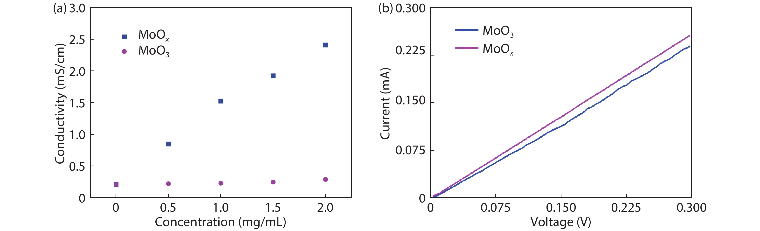
The conductivity of HTL films with 0–2 mg/mL MoOx doped in PEDOT:PSS was tested using a four-point probe (Fig. 1(a)). Deposition and measurement of the films were performed in atmosphere under conditions. A significant increase in conductivity from 2.1 × 10⁻⁴ to 2.4 × 10⁻³ S/cm was observed. In addition, the conductivity of PEDOT:PSS-MoOx was obviously better than that of the PEDOT:PSS-MoO3. This indicates that the enhanced conductivity of HTL films is linear to MoOx concentration. It is well-known that the number of O vacancies in MoOx is larger than that of fully stoichiometric configuration of MoO3. Therefore, the fact of enhancing conductivity of PEDOT:PSS-MoOx is consistent to the previous report that the O vacancies determine the conductivity of MoOx[
![]()
Figure 1.(Color online) (a) The in-plane conductivity of HTL films with 0–2 mg/mL MoO
To further prove the presence of O vacancies in MoOx, the chemical composition of the MoOx and MoO3 was probed using X-ray photoelectron spectroscopy (XPS), as shown in Fig. 2. From Fig. 2(a) it can be seen that the major species Mo6+ was present in MoO3. The Mo 3d peak was deconvoluted to obtain the contributions of Mo5+ (232.0 eV for Mo 3d5/2) and Mo6+ (232.7, 236.0 eV) and the major species present in MoOx is the mixture of Mo5+ and Mo6+, as shown in Fig. 2(b). In addition, Mo5+ species was found to be 18.7 atomic rations (%). Mo5+ species is the origin of the metal-like electrical properties of MoOx, which could low the series resistance of solar cell, and be beneficial to collect photo-generated charge carriers and finally enhance Jsc of solar cells.
![]()
Figure 2.(Color online) XPS profiles of (a) MoO3 and (b) MoO
2.3. Device fabrication
The conventional planar architecture is adopted to further prove the effect of MoOx on the performance of hybrid PSCs, which is constructed with indium tin oxide (ITO)/HTL/CH3NH3PbI3–xClx/PC61BM/Bphen/Ag (Fig. 3(a)). The PEDOT:PSS-MoOx, PEDOT:PSS-MoO3, and PEDOT:PSS were used to fabricate the HTLs. The performance of the devices with these three different HTLs is investigated under AM 1.5 G 100 mW/cm2 illumination. According to our previous work[
![]()
Figure 3.(Color online) (a) Device construction of the planar PSCs, and (b) cross-sectional SEM image of the planar PSC structures without an Ag electrode.
3. Results and discussion
The current density–voltage (J–V) characteristics of PSCs using the different HTLs are shown in Fig. 4(a). The relevant performance parameters are also summed up in the inset of Fig. 4(a). Figure 4(b) shows the histogram of PSCs using PEDOT:PSS-MoOx and PEDOT:PSPS-MoO3. The device with HTL of PEDOT:PSS exhibited a PCE of 11.04%, with Voc of 0.96 V, Jsc of 17.75 mA/cm2, and FF of 0.65. The device with HTL of PEDOT:PSS-MoO3 shows a significantly enhanced PCE of 12.75% with a Voc of 1.01 V, Jsc of 18.22 mA/cm2, and FF of 0.70. Compared to that of the PEDOT:PSS-MoO3 device, the PCE of the PEDOT:PSS-MoOx device furthermore improved from 12.75 to 15.01%.
![]()
Figure 4.(Color online) (a) The best
By analyzing the data shown in the inset of Fig. 5, we can also see that the FF and Jsc values are improved and the series resistances (Rs) are reduced. The values of Rs of the PEDOT:PSS-based cells, PEDOT:PSS-MoO3, and PEDOT:PSS-MoOx are 18.65, 16.89, and 3.89 Ω·cm2, respectively. The use of MoO3 NPs additive induces oxidation doping of PEDOT:PSS, which promotes the networking between the conducting PEDOT units, and thereby greatly increases the electric conductivity of hybrid PEDOT:PSS-MoO3 and PEDOT:PSS-MoOx layer[
![]()
Figure 5.(Color online) Average photovoltaic parameter for 12 devices: (a) open-circuit voltage (
It is supposed that the significant reduction of Rs ascribes to the good conductivity of PEDOT:PSS-MoOx, and the high hole-conductivity could result in the high Jsc and the high FF due to the reduced Rs, which corresponds to the previous report by Nguyen et al.[
The obvious increase of Jsc could be attributed to the incorporation of MoOx into HTLs and the reduced Rs. Pristine PEDOT:PSS is a poor conductor, resulting in the low charge collection efficiency due to charge reorganization which dominates the charge transfer[
The addition of Mo5+ caused the conductivity of the HTL to increase, which resulted in a decrease of Rs, and the reduced Rs greatly affected FF, thus getting an increase in FF[
To further verify what caused the improvements on FF and Jsc, the atomic force microscopy (AFM) images and SEM images were carried out to research the surface properties of the HTLs and the perovskite layers. Fig. S1 displays AFM images of the PEDOT:PSS-MoO3 and PEDOT:PSS-MoOx, as well as SEM images of perovskite layers on the PEDOT:PSS-MoO3 and PEDOT:PSS-MoOx. The PEDOT:PSS-MoO3 and PEDOT:PSS-MoOx interface modification had a little effect on the morphology of perovskite films but it is not so obvious. The identical XRD patterns observed from the perovskite films indicated that perovskite crystallizations on PEDOT:PSS-MoO3 and PEDOT:PSS-MoOx were the same (Fig. S2). Thus, the difference of photovoltaic performance was solely caused by the different Mo valence states.
To understand the effect of Mo5+ on the resistance of the device, Impedance Spectroscopy (IS) measurements were carried out under dark conditions, which provided insights on the charge transport, recombination, and accumulation within the perovskite-based devices[
![]()
Figure 6.(Color online) Nyquist plot of devices with various HTLs (pristine PEDOT:PSS, PEDOT:SS-MoO
The single semicircle appears in Fig. 6, which is consistent with expectation. Moreover, the semi-arc gets smaller as the addition of Mo5+ into PEDOT:PSS. We attributed this result to the occupancy of the trap states at the perovskite/HTL interface, which is associated with the presence of a capacitance (Cp)[
We demonstrated the improved photovoltaic performance by using highly conductive HTLs, namely PEDOT:PSS-MoOx. Therefore, we will discuss the possible mechanisms for improved performance from the molecular design perspective.
The open-circuit photovoltage decay (OCVD) measurements are to establish a photo-stationary state, and the device is illuminated during open circuit[
![]()
Figure 7.(Color online) (a) OCVD measurements for three types of devices. (b) Schematic of the proposed mechanism for the trap-assisted recombination.
It is well known that the charge density in the device is closely related to Voc with the following equation:
which is supposed that the photovoltage is equal to the quasi Fermi level splitting[
The dielectric constants εr of the perovskite device based on PEDOT:PSS-MoO3 and PEDOT:PSS-MoOx, are tested showed as Fig. 8(a), and the characteristic behavior of the frequency is the real part of the dielectric constant. In low frequency, a significant increase of εr of the perovskite device based on PEDOT:PSS-MoOx is produced compared to that of PEDOT:PSS-MoO3. At low frequencies—namely, below 106 Hz—the dielectric response, εr, was assumed to be an ionic conduction, which largely stems from the accumulation of electrode interface charge. In the high-frequency zone, the change of εr value is mainly caused by the electronic conduction[
![]()
Figure 8.(Color online) (a) Real part of the dielectric constant as a function of frequency in the dark. (b) Schematic diagram of electric-field distribution in the perovskite device based on PEDOT:PSS-MoO
The εr also affected the recombination of charges in the interface between the perovskite and the HTL. The holes were captured and ended up by the Coulombic interactions between the holes and the negatively charged trap states on the perovskite surface. The trap-assisted reorganization process takes place between the perovskite layer and HTL, as shown by Fig. 7(b). The critical distance (rc) can be expressed as follows:
where q, ε0, εr, and T are the elementary charge, vacuum permittivity, the dielectric constant of HTL, and temperature, respectively[
To further distinguish the dielectric constant effect on the polarization performance, the J–V curves of the same device at the different scanning directions were performed in the dark as shown in Fig. 8(c), which could also explain the possible effect mechanism of interfacial polarization on charge recombination in PSCs. Interfacial polarization was tested with an external bias, as shown in Fig. 8(b). The applied external bias is ranged from 0 to 0.3 V, and J–V curves were obtained for both devices containing PEDOT:PSS-MoOx and PEDOT:PSS-MoO3.
Apart from the impact of MoOx on conductivity of PEDOT:PSS, the current effect at the different directions of the applied DC field is also studied. The device with a positive electrode linked to a test anode had a similar electron transfer direction to PSC of PEDOT:PSS-MoOx and PEDOT:PSS-MoO3. In contrast, a device with a positive electrode linked to a test cathode had an electron transfer direction opposite the two devices. It can be seen from Fig. 8(b) that the measured current and the applied bias are positive correlation. After changing the direction of the applied field, it is found that the current of PSC based on PEDOT:PSS-MoO3 is very similar to the current before the applied field is changed in the total applied field range. This result suggests that the charge transport in PSC based on PEDOT:PSS-MoO3 makes no change. Once MoO3 is changed to MoOx (with the same electron transfer direction and applied DC power source), the interface induced polarization initiates the electron-hole dipole pairs to separate, then the current is increased. After the direction of the applied field was changed, the current was observed to be measured at room temperature and 0 V applied bias for the perovskite devices based on PEDOT:PSS-MoOx. The current is lower than that with a positive field in the overall applied field range. This could be clarified to be the significant contribution of interface induced polarization between the perovskite and PEDOT:PSS-MoOx. When both of the electron transfer directions from the applied DC power source and the interface effect are identical, interface induced polarization initiating the separation of electron-hole dipole pairs could contribute to the increasing current. Fig. 8(c) shows a schematic diagram of electric field distribution in perovskite device based on PEDOT:PSS-MoOx. The polarization field (Ep) was consistent with the internal built field (E0). Therefore, it facilitated the separation of photo generated holes and electrons. The accumulated photo-generated holes first at the perovskite/HTL interface are dragged into the PEDOT:PSS-MoOx layer by Ep and then extracted at the anode, and this reduces the probability of non-radiative recombination by surface and bulk traps in the perovskite layer[
4. Conclusion
We have revealed and highlighted the important effect of Mo5+ on the conductivity and polarization of HTLs using PSCs. The enhanced conductivity of the HTL by incorporating Mo5+ into PEDOT:PSS HTL significantly boosted the photocurrent and reduced charge recombination, which effectively improved device PCES due to the manipulation of the hole pathway by using the more electrically conductive MoOx and the dielectric constant. We speculated that the higher dielectric constant can produce a polarization field and screen the reorganisation of the traps and the holes in the extraction layer, which could potentially reduce photogenerated charge recombination in the interface of the perovskite and the HTLs. This discovery affords an effective strategy for structuring efficient charge-transport materials to increase the overall performance of PSCs.
Acknowledgements
This work was supported by Colleges Universities in Henan Province Key Scientific Research Project Funding Scheme (No. 17A140020), Henan Province Nature Science Foundation Project (No. 182300410241) and Chinese Nature Science Foundation Committee (No. 61640406).
References
[1] S De Wolf, J Holovsky, S J Moon et al. Organometallic halide perovskites: sharp optical absorption edge and its relation to photovoltaic performance. J Phys Chem Lett, 5, 1035(2014).
[2] G Xing, N Mathews, S Sun et al. Long-range balanced electron-and hole-transport lengths in organic-inorganic CH3NH3PbI3. Science, 342, 344(2013).
[3] H Yoon, S M Kang, J K Lee et al. Hysteresis-free low-temperature-processed planar perovskite solar cells with 19.1% efficiency. Energy Environ Sci, 9, 2262(2016).
[4] G Xing, N Mathews, S S Lim et al. Low-temperature solution-processed wavelength-tunable perovskites for lasing. Nat Mater, 13, 476(2014).
[5] J H Heo, S H Im, J H Noh et al. Efficient inorganic–organic hybrid heterojunction solar cells containing perovskite compound and polymeric hole conductors. Nat Photonics, 7, 486(2013).
[6] D Bryant, P Greenwood, J Troughton et al. A transparent conductive adhesive laminate electrode for high-efficiency organic-inorganic lead halide perovskite solar cells. Adv Mater, 26, 7499(2014).
[7] Q Jiang, L Zhang, H Wang et al. Enhanced electron extraction using SnO2 for high-efficiency planar-structure HC(NH2)2PbI3-based perovskite solar cells. Nat Energy, 2, 1(2016).
[8] N Aeineh, E M Barea, A Behjat et al. Inorganic surface engineering to enhance perovskite solar cell efficiency. ACS Appl Mater Interfaces, 9, 13181(2017).
[9] V Gonzalez-Pedro, E J Juarez-Perez, W S Arsyad et al. General working principles of CH3NH3PbX3 perovskite solar cells. Nano Lett, 14, 888(2014).
[10] K Yang, J Fu, L Hu et al. Impact of ZnO photoluminescence on organic photovoltaic performance. ACS Appl Mater Interfaces, 10, 39962(2018).
[11]
[12] J Xie, X Yu, X Sun et al. Improved performance and air stability of planar perovskite solar cells via interfacial engineering using a fullerene amine interlayer. Nano Energy, 28, 330(2016).
[13] H Kim, K G Lim, T W Lee. Planar heterojunction organometal halide perovskite solar cells: roles of interfacial layers. Energy Environ Sci, 9, 12(2016).
[14] Z K Wang, X Gong, M Li et al. Induced crystallization of perovskites by a perylene underlayer for high-performance solar cells. ACS Nano, 10, 5479(2016).
[15] X Liu, B Li, N Zhang et al. Multifunctional RbCl dopants for efficient inverted planar perovskite solar cell with ultra-high fill factor, negligible hysteresis and improved stability. Nano Energy, 53, 567(2018).
[16] L Hu, M Li, K Yang et al. PEDOT:PSS monolayers to enhance the hole extraction and stability of perovskite solar cells. J Mater Chem A, 6, 16583(2018).
[17] M Qian, M Li, X B Shi et al. Planar perovskite solar cells with 15.75% power conversion efficiency by cathode and anode interfacial modification. J Mater Chem A, 3, 13533(2015).
[18] L Zhao, D Luo, J Wu et al. High-performance inverted planar heterojunction perovskite solar cells based on lead acetate precursor with efficiency exceeding 18%. Adv Funct Mater, 26, 3508(2016).
[19] E J Juarez-Perez, M Wuβler, F Fabregat-Santiago et al. Role of the selective contacts in the performance of lead halide perovskite solar cells. J Phys Chem Lett, 5, 680(2014).
[20] V W Bergmann, S A Weber, F J Ramos et al. Real-space observation of unbalanced charge distribution inside a perovskite-sensitized solar cell. Nat Commun, 5, 5001(2014).
[21] A Abrusci, S D Stranks, P Docampo et al. High-performance perovskite-polymer hybrid solar cells via electronic coupling with fullerene monolayers. Nano Lett, 13, 3124(2013).
[22] W Tress, N Marinova, T Moehl et al. Understanding the rate-dependent
[23] X Crispin, F L Jakobsson, A Crispin et al. The origin of the high conductivity of poly (3, 4-ethylenedioxythiophene)− poly (styrenesulfonate)(PEDOT−PSS) plastic electrodes. Chem Mater, 18, 4354(2006).
[24] X Zheng, Y Bai, S Xiao et al. Strategies for improving efficiency and stability of perovskite solar cells. MRS Adv, 2, 3051(2017).
[25] X Huang, K Wang, C Yi et al. Efficient perovskite hybrid solar cells by highly electrical conductive PEDOT:PSS hole transport layer. Adv Energy Mater, 6, 1501773(2016).
[26] I Anusca, S Balčiūnas, P Gemeiner et al. Dielectric response: answer to many questions in the methylammonium lead halide solar cell absorbers. Adv Energy Mater, 7, 1700600(2017).
[27] Y Jiang, C Li, H Liu et al. Poly (3, 4-ethylenedioxythiophene): poly (styrenesulfonate)(PEDOT:PSS) –molybdenum oxide composite films as hole conductors for efficient planar perovskite solar cells. J Mater Chem A, 4, 9958(2016).
[28] Z Wang, Y Lou, S Naka et al. Direct comparison of solution- and vacuum-processed small molecular organic light-emitting devices with a mixed single layer. ACS Appl Mater Interfaces, 3, 2496(2011).
[29] P Schulz, J O Tiepelt, J A Christians et al. High-work-function molybdenum oxide hole extraction contacts in hybrid organic–inorganic perovskite solar cells. ACS Appl Mater Interfaces, 8, 31491(2016).
[30] H S Kim, J B Cook, H Lin et al. Oxygen vacancies enhance pseudocapacitive charge storage properties of MoO3−
[31] M H Lee, L Chen, N Li et al. MoO3-induced oxidation doping of PEDOT: PSS for high performance full-solution-processed inverted quantum-dot light emitting diodes. J Mater Chem C, 5, 10555(2017).
[32] W H Nguyen, C D Bailie, E L Unger et al. Enhancing the hole-conductivity of spiro-OMeTAD without oxygen or lithium salts by using spiro (TFSI)2 in perovskite and dye-sensitized solar cells. J Am Chem Soc, 136, 10996(2014).
[33] N Wang, K Zhao, T Ding et al. Improving interfacial charge recombination in planar heterojunction perovskite photovoltaics with small molecule as electron transport layer. Adv Energy Mater, 7, 1700522(2017).
[34] Z Li, J Tinkham, P Schulz et al. Acid additives enhancing the conductivity of Spiro-OMeTAD toward high-efficiency and hysteresis-less planar perovskite solar cells. Adv Energy Mater, 7, 1601451(2017).
[35] Y Shao, Y Yuan, J Huang. Correlation of energy disorder and open-circuit voltage in hybrid perovskite solar cells. Nat Energy, 1, 1(2016).
[36] A Dualeh, T Moehl, N Tétreault et al. Impedance spectroscopic analysis of lead iodide perovskite-sensitized solid-state solar cells. ACS Nano, 8, 362(2014).
[37] A Pockett, G E Eperon, T Peltola et al. Characterization of planar lead halide perovskite solar cells by impedance spectroscopy, open-circuit photovoltage decay, and intensity-modulated photovoltage/photocurrent spectroscopy. J Phys Chem C, 119, 3456(2015).
[38] A M Humada, M Hojabri, S Mekhilef et al. Solar cell parameters extraction based on single and double-diode models: A review. Renew Sustain Energy Rev, 56, 494(2016).
[39] F Tan, S Qu, Q Jiang et al. Interpenetrated inorganic hybrids for efficiency enhancement of PbS quantum dot solar cells. Adv Energy Mater, 4, 1400512(2014).
[40] Z Liu, S Niu, N Wang. Light illumination intensity dependence of photovoltaic parameter in polymer solar cells with ammonium heptamolybdate as hole extraction layer. J Colloid Interface Sci, 509, 171(2018).
[41] A Baumann, K Tvingstedt, M C Heiber et al. Persistent photovoltage in methylammonium lead iodide perovskite solar cells. Appl Mater, 2, 081501(2014).
[42] F Tan, H Tan, M I Saidaminov et al. In situ back-contact passivation improves photovoltage and fill factor in perovskite solar cells. Adv Mater, 31, 1807435(2019).
[43] Y Shao, Z Xiao, C Bi et al. Origin and elimination of photocurrent hysteresis by fullerene passivation in CH3NH3PbI3 planar heterojunction solar cells. Nat Commun, 5, 5784(2014).
[44] L Hu, K Sun, M Wang et al. Inverted planar perovskite solar cells with a high fill factor and negligible hysteresis by the dual effect of NaCl-doped PEDOT: PSS. ACS Appl Mater Interfaces, 9, 43902(2017).
[45] M Kuik, L J Koster, G A Wetzelaer et al. Trap-assisted recombination in disordered organic semiconductors. Phys Rev Lett, 107, 256805(2011).
[46] D Sapori, M Kepenekian, L Pedesseau et al. Quantum confinement and dielectric profiles of colloidal nanoplatelets of halide inorganic and hybrid organic–inorganic perovskites. Nanoscale, 8, 6369(2016).
[47] T M Brenner, D A Egger, L Kronik et al. Hybrid organic–inorganic perovskites: low-cost semiconductors with intriguing charge-transport properties. Nat Rev Mater, 1, 1(2016).

Set citation alerts for the article
Please enter your email address
© Copyright 2018-2021 | Chinese Laser Press. All Rights Reserved 沪ICP备15018463号-20