Abstract
Tungsten telluride thin films were successfully prepared on monocrystal sapphire substrates by using atomic layer deposition and chemical vapor deposition technology, and the effects of different tellurization temperatures on the properties of tungsten telluride films were investigated. The growth rate, crystal structure and composition of the film samples were characterized and analyzed by using scanning electron microscope, Raman spectroscopy and X-ray photoelectron spectroscopy. The results showed that tungsten telluride thin films with good crystal orientation in (001) were obtained at telluride temperature of 550 °C. When the telluride temperature reached 570 °C, the tungsten telluride began to decompose and unsaturated magnetoresistance was found.Tungsten telluride thin films were successfully prepared on monocrystal sapphire substrates by using atomic layer deposition and chemical vapor deposition technology, and the effects of different tellurization temperatures on the properties of tungsten telluride films were investigated. The growth rate, crystal structure and composition of the film samples were characterized and analyzed by using scanning electron microscope, Raman spectroscopy and X-ray photoelectron spectroscopy. The results showed that tungsten telluride thin films with good crystal orientation in (001) were obtained at telluride temperature of 550 °C. When the telluride temperature reached 570 °C, the tungsten telluride began to decompose and unsaturated magnetoresistance was found.Introduction
Two-dimensional topological insulators, also known as quantum spinning Hall insulators, have edge states protected by topology[1]. Because this channel can support non-dissipative electron transmission, it is expected to achieve the next generation of low-loss electronic devices and has been widely studied[2-4]. Since 2006, the Zhang team from Stanford University predicted the existence of quantum spinning Hall effect (quantum spin Hall effect, QSH) in HgTe/CdTe quantum wells[5]. In the following year, the experiments of Molenkamp team from the Institute of Physics of the University of Wurzburg confirmed it[6]. Researchers have carried out a large number of theoretical predictions and experimental explorations to find more practical natural QSH materials[7-9]. Compared with complex quantum well structures, natural QSH materials have advantages in sample preparation and heterojunction device construction. However, it is still very difficult to realize QSH effect in a natural monolayer two-dimensional system. Top-down mechanical stripping and bottom-up epitaxial growth are two common methods to successfully prepare monolayer QSH materials.
WTe2 is a unique semi-metal with a small and complex Fermi surface, which has the properties of unsaturated magnetoresistance[10], high voltage superconductivity, linear magnetoresistance and anisotropic magnetoresistance[11-14]. It can be used in channel materials of field effect transistors and solar cells. The edge states of monolayer 1T'-WTe2 thin films are verified by various non-local transport tests[15,16], and the edge channels show a quantized conductance value 2e2/h within 100 nm length[16]. However, when the length limit is exceeded, the conductance of the edge channel begins to decrease. One of the main reasons for this phenomenon is that the intrinsic monolayer 1T'-WTe2 is semi-metallic and lacks an insulation energy gap[7,17,18].
At present, there are two kinds of preparation methods of tungsten ditelluride, including top-down methods such as mechanical stripping method, which suffer from problems such as small size and poor uniformity, and bottom-top method, such as molecular beam epitaxy, chemical vapor deposition and so on. These methods often require a high temperature above 800 °C and cannot control the thickness uniformity of the film. Therefore, a new and simple method to prepare large area, uniform and high quality 1T'-WTe2 is very important.
In this paper, tungsten telluride thin films were prepared by atomic layer deposition (ALD) and chemical vapor deposition (CVD). ALD process has the advantages of self-limiting, excellent three-dimensional shape preservation, large area uniformity and accurate film thickness control, which is very useful in devices requiring conformal and thickness requirements. Tungsten telluride thin films with large size, few defects and high crystallinity were prepared by two-step method based on the controllable thickness and large area uniformity of ALD. At the same time, the effects of telluride temperature on the composition of tungsten telluride films and the effects of film oxidation on the composition and magnetic properties of tungsten telluride films were studied.
Experiments and tests
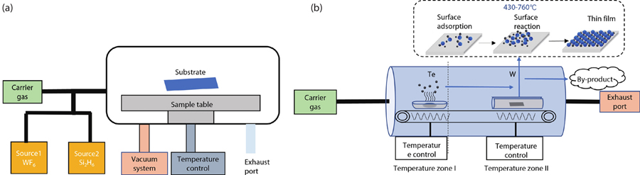
Tungsten ditelluride was prepared by ALD and CVD two-step method. The ALD system is the TALD-100 equipment of Jiaxing Kemin Electronic Equipment Technology Co., Ltd., the 2-inch sapphire substrate with orientation (0001) is used, the background vacuum is less than 10–4 Torr, tungsten hexafluoride (WF6, with 99.99% purity) and ethylsilane (Si2H6, with 99.99% purity) are used as precursors, high purity Ar (99.999%) is used as carrier gas, and the vacuum in the cavity is kept at 0.15 Torr. The growth temperature of the film is controlled at 200 °C. The flow rate and pressure of WF6 and Si2H6 are regulated by the regulator of anti-corrosive gas. The deposition formula is as follows: 0.05 s Si2H6 pulse time, 10 s reaction time, 60 s purge time, 0.05 s WF6 pulse time, 10 s reaction time and 60 s purge time. The time of adding reaction to the formula is to make the precursor fully and uniformly adsorb to the substrate surface. Tungsten films were obtained by the growth of 40 and 100 cycles.
The tungsten film was tellurized in the CVD equipment. The CVD system was the CVD-2 equipment of Jiaxing Kemin Electronic Equipment Technology Co., Ltd., which had the function of double temperature zone control. Some excessive tellurium blocks were placed in the quartz boat, the sapphire substrate with tungsten film was cut into 8 × 10 mm2 size, and the quartz boat and tungsten film were placed in two temperature zone I and II, respectively (Fig. 1). The temperature in zone I rose to 550 °C at 100 min, and the temperature in zone II rose to telluride temperature at 100 min. The telluride temperature was set at 430–760 °C through the temperature control module to study the effect of telluride temperature. A 10% Ar/H2 mixture of 100 sccm passed through zone I and II in turn as carrier gas, and then cooled naturally to room temperature after holding for 100 min.

Figure 1.(Color online) (a) Schematic diagram of ALD device. (b) Schematic diagram of CVD device.
Scanning electron microscope (SEM) and energy dispersive spectroscopy (EDS) were tested by Japanese Hitachi SU5000 thermal field emission scanning electron microscope. Atomic force microscopy (AFM) was tested by German Burker Dimension ICON AFM. X-ray photoelectron spectroscopy (XPS) was tested by American ThermoFisher ESCALAB XI+X-ray photoelectron spectrometer. X-ray diffraction (XRD) was tested by German Bruker D2 PHASER X-ray diffractometer, and Raman was tested by German WITec alpha300R rapid Raman imaging spectrometer in 532 nm. The magnetoresistance was tested by Quantum design physical property measurement system (PPMS).
Results and discussions
The cross section of W thin films deposited by ALD tested by SEM showed that the thickness of 100 cycle deposition was 72.57 nm (Fig. 2(a)), indicating the growth rate of ALD was 7.2 Å/cycle. XPS spectrum of W film deposited by ALD showed that there were peaks of W and WO3 in the spectrum (Fig. 2(b)), indicating that the film was a mixture of W and WO3. Since the precursors were Si2H6 and WF6, and there was no oxygen element. WO3 may be caused by the water vapor adsorbed in the chamber of the equipment participating in the reaction, or by the partial oxidation of the W film exposed to air. W thin films were cut into 8 × 10 mm2 and tellurized to obtain WTe2 thin films (Fig. 2(c)).
Figure 2.(Color online) (a) SEM image of cross section of tungsten thin film. (b) The XPS pattern of tungsten thin film. (c) The photo of tungsten film.
To study the effect of telluride temperature on tellurization, the Raman spectrum were obtained at 430, 470, 550, 560, 570, 580 and 760°C. The Raman spectrum showed seven main peaks at 81, 88, 110, 115, 132, 162 and 211 cm–1[19-21], corresponding to the vibration modes of
,
,
,
,
,
and
, respectively (Fig. 3(a)). The peaks of
,
and
at 430 and 470 °C were not obvious, and the heat of formation of H2Te is –146.4 kJ/mol. This may be due to the low telluride temperature and the limitation of chemical vapor reaction rate, although sufficient tellurium entered the tungsten film, it did not react with tungsten. Tungsten telluride decomposed by releasing Te vapor at high temperature (about 600 °C). When the telluride temperature reaches 760 °C, the tungsten telluride decomposed, resulting in the disappearance of the Raman peak of tungsten telluride.
Figure 3.(Color online) (a) Raman spectrum at different telluride temperatures. (b) Te : W ratio-temperature curves in EDS results
Because the electronegativity difference between Te and W was small (about 0.4 eV)[22], the bonding between Te and W was weak, it was difficult to obtain Te : W tungsten ditelluride at 2 : 1 stoichiometry, and the activity of Te was low, while tungsten telluride decomposed by releasing Te vapor at high temperature (about 600 °C), so Te was reduced to intermediate hydrogen telluride by H2 at atmospheric pressure, which made it easier for H2Te to react with W thin films.
The Te : W ratios under various temperature were tested by EDS (Fig. 3(b)). When the telluride temperature is 430 and 470 °C, Te : W was 2.31 and 2.5 (Fig. 3(b)). It was attributed to the lower reaction temperature and the excessive Te entered the W film without reacting with W. With the increase of temperature, the atomic ratio of Te : W decreased gradually. When the temperature was 570 and 580 °C, Te : W was 1.9 and 1.89, indicating that the formed tungsten telluride may be partially decomposed, resulting in the decrease of Te. When the temperature was 550 and 560 °C, Te : W was 2.03 (1.97), which was close to the theoretical value 2. This indicates that the telluride films conformed to the stoichiometric ratio when the telluride temperature was between 550 and 580 °C.
Figs. 4(b) and4(c) show the XRD spectrum at 550 and 560 °C tellurization temperature. The diffraction peak matched well with (002) (004) (006) (008) crystal plane diffraction peak of tungsten telluride[23]; that is, WTe2 had a better crystal preferred orientation at (00l). The XRD peak value corresponding to 550°C telluride temperature inFig. 4(b) was larger and had a narrower half-peak width, indicating that the crystallinity was better at 550 °C tellurization temperature. At the same time, no diffraction peak of WO3–x was found in the XRD results, indicating that the oxidized tungsten was also completely tellurized into tungsten telluride, the exposure time in air was short, and no oxidation occurred. However, the diffraction peaks of WO3 and W were found inFig. 4(a)[24], indicating that there were still some tungsten films without tellurization reaction at 470 °C[25]. Some diffraction peaks belonging to W were found inFig. 4(d). The tungsten telluride had been partially decomposed and Te overflowed at 580 °C, which was consistent with the conclusion of Te : W < 2 in EDS results. The result showed that the FWHM of (002) is 0.1966° at 550 °C (Fig. 4(e)), indicated better crystallinity.
Figure 4.(a–d) XRD curves of telluride temperature at 470, 550, 560 and 580 °C. (e) FWHM of WTe2(002) at 470, 550, 560 and 580 °C.
To analyze the composition and valence state of the sample at 550 °C, the sample was tested by XPS.Fig. 5(a) gives the spectrum of W4f, the binding energy was located at 31.7 and 33.7 eV corresponding to the W peak of W4+4f7/2 and W4+4f5/2, respectively,Fig. 5(b) gives the XPS spectrum of Te 3d[26], and the binding energy at 583.6 and 572.6 eV corresponded to Te2– 3d3/2 and Te2– 3d5/2, respectively, which could be attributed to the W–Te bond and proves that the resulting thin film was tungsten telluride.
Figure 5.(Color online) (a) The XPS curve of the sample at 550°C. (b) The schematic diagram of oxidation principle. (c) The oxidation principle diagram.
In theFig. 5(a), the binding energies at 35.9 and 37.8 eV corresponded to W4f7/2 and W4f5/2, respectively, which could be attributed to the vibration of the W–O bond[24-28]. InFig. 3(b), the Te4+ peak of binding energy at 587.4 and 576 eV could be attributed to the vibration of the Te–O bond[29,30], which was caused by the easy oxidation of tungsten telluride in air. Tungsten telluride was extremely sensitive to the environment.Fig. 5(c) gives the oxidation principle diagram. The sites shown in the diagram were highly exothermic (ΔEads = –3.6 eV/O2) during the adsorption process[19], which was beneficial to the dissociation and adsorption of oxygen[3]. When oxygen dissociated, one oxygen atom bound directly to the W atom, and the other oxygen atom replaced tellurium to form a W3O subunit corresponding to the W–O vibration in XPS.
The comprehensive physical properties of the samples tellurized at 550 °C were tested.Fig. 6(a) shows the resistance-temperature curve of tungsten telluride thin films from 2 to 300 K without external magnetic field. The results show that the resistance decreased with the increase of temperature, that was, the prepared tungsten telluride thin films were insulated. This is consistent with the previously reported results[19], which were attributed to the oxidation of tungsten telluride.
Figure 6.(Color online) (a)R–T curve and (b) MR curve of tungsten telluride thin films at 550 °C tellurization temperature.
Define MR = (ρ(B)–ρ(0))/ρ(0) × 100%.Fig. 6(b) shows that MR was 3.8% and 3.4% at 5 and 7 K temperature under 15 T magnetic field, respectively. Although the magnetoresistance was very small, there was no saturation trend at low temperature[31-33]. At 1.9 K low temperature, MR could reach 112.8%. The MR is less than 300% of the reported maximum magnetoresistance (XMR)[21], which may be due to the exposure and oxidation of tungsten telluride thin films in air. Due to oxidation, the WO3–x formed on the surface of WTe2 acted as a hole donor, which destroyed the perfect compensation of electron holes and greatly reduced XMR. However, because the surface oxidation was self-limiting, the thicker the thickness was, the more difficult the oxidation was, and so the decrease of MR tended to be stable with the increase of exposure time. Nevertheless, the test still showed that the tungsten telluride thin films grown at 550 °C had large unsaturated magnetoresistance.
Summary
To obtain WTe2 thin films with excellent crystallinity, W simple-substance thin films were prepared by ALD and CVD two-step methods, and were then tellurized at different telluride temperatures. Tungsten telluride thin films with good crystal orientation were obtained at 550 °C. At the same time, the effect of telluride temperature on the tellurization reaction was studied. It was found that the telluride temperature was low and the chemical vapor reaction rate was limited. When the telluride temperature reached 570 °C, tungsten telluride began to decompose. Through the test of its electromagnetic properties, the phenomenon of unsaturated magnetoresistance was found. It was found that the tungsten telluride film was in an insulated state and the MR was small due to the exposure of tungsten telluride to air oxidation.
Because of the self-limiting of ALD, good thickness control could be achieved. Through thinning of W single-substance thin films by ALD technology, tungsten films could be further thinned and the thickness of tungsten films could be controlled at the atomic level. Through the research and control of temperature, the growth of tungsten telluride thin films with different thickness could be realized, which would be of great significance for the preparation of uniform large area tungsten telluride thin films with controllable thickness, and provides new ideas and methods for the preparation of two-dimensional tungsten telluride thin films.
References
[1] X L Qi, S C Zhang. Topological insulators and superconductors. Rev Mod Phys, 83, 1057(2011).
[2] B Ghosh, A Gupta, B Bishnoi. Effects of defects on the electronic properties of WTe2 armchair nanoribbons. J Semicond, 35, 113002(2014).
[3] Z Q Zhou, Y Cui, P H Tan et al. Optical and electrical properties of two-dimensional anisotropic materials. J Semicond, 40, 061001(2019).
[4] P Zhang, Y W Zhang, Y Wei et al. Contact engineering for two-dimensional semiconductors. J Semicond, 41, 071901(2020).
[5] B A Bernevig, T L Hughes, S C Zhang. Quantum spin Hall effect and topological phase transition in HgTe quantum wells. Science, 314, 1757(2006).
[6] M König, S Wiedmann, C Brüne et al. Quantum spin hall insulator state in HgTe quantum wells. Science, 318, 766(2007).
[7] X F Qian, J W Liu, L Fu et al. Quantum spin Hall effect in two-dimensional transition metal dichalcogenides. Science, 346, 1344(2014).
[8] C C Liu, W X Feng, Y G Yao. Quantum spin Hall effect in silicene and two-dimensional germanium. Phys Rev Lett, 107, 076802(2011).
[9] Y Xu, B H Yan, H J Zhang et al. Large-gap quantum spin hall insulators in tin films. Phys Rev Lett, 111, 136804(2013).
[10] M N Ali, J Xiong, S Flynn et al. Large, non-saturating magnetoresistance in WTe2. Nature, 514, 205(2014).
[11] Y K Luo, H Li, Y M Dai et al. Hall effect in the extremely large magnetoresistance semimetal WTe2. Appl Phys Lett, 107, 182411(2015).
[12] Y Song, Q Zhang, W B Mi et al. Valley polarization and p-/n-type doping of monolayer WTe2 on top of Fe3O4(111). Phys Chem Chem Phys, 18, 15039(2016).
[13] Z W Zhu, X Lin, J Liu et al. Quantum oscillations, thermoelectric coefficients, and the Fermi surface of semimetallic WTe2. Phys Rev Lett, 114, 176601(2015).
[14] J Jiang, F Tang, X C Pan et al. Signature of strong spin-orbital coupling in the large nonsaturating magnetoresistance material WTe2. Phys Rev Lett, 115, 166601(2015).
[15] Z Y Fei, T Palomaki, S F Wu et al. Edge conduction in monolayer WTe2. Nat Phys, 13, 677(2017).
[16] S F Wu, V Fatemi, Q D Gibson et al. Observation of the quantum spin Hall effect up to 100 kelvin in a monolayer crystal. Science, 359, 76(2018).
[17] Y H Song, Z Y Jia, D Q Zhang et al. Observation of Coulomb gap in the quantum spin Hall candidate single-layer 1T’-WTe2. Nat Commun, 9, 4071(2018).
[18] Z Y Jia, Y H Song, X B Li et al. Direct visualization of a two-dimensional topological insulator in the single-layer 1T'-WTe2. Phys Rev B, 96, 041108(2017).
[19] J Li, S Cheng, Z X Liu et al. Centimeter-scale, large-area, few-layer 1T'-WTe2 films by chemical vapor deposition and its long-term stability in ambient condition. J Phys Chem C, 122, 7005(2018).
[20] Y C Jiang, J Gao, L Wang. Raman fingerprint for semi-metal WTe2 evolving from bulk to monolayer. Sci Rep, 6, 19624(2016).
[21] J D Zhou, F C Liu, J H Lin et al. 2D materials: Large-area and high-quality 2D transition metal telluride. Adv Mater, 29, 1603471(2017).
[22] Y Zhou, H Jang, J M Woods et al. Direct synthesis of large-scale WTe2 thin films with low thermal conductivity. Adv Funct Mater, 27, 1605928(2017).
[23] Aslan T, Mtsuko D, Coleman C, et al. Observation of Shubnikov de Haas and aharanov-bohm oscillations in silicon nanowires. arXiv: 1504.02325, 2015
[24] Y Wang, X Wang, Y Xu et al. Simultaneous synthesis of WO3–x quantum dots and bundle-like nanowires using a one-pot template-free solvothermal strategy and their versatile applications. Small, 11, 1310(2017).
[25] W Lu, Y D Zhang, Z S Zhu et al. Thin tungsten telluride layer preparation by thermal annealing. Nanotechnology, 27, 414006(2016).
[26] C H Naylor, W M Parkin, Z L Gao et al. Large-area synthesis of high-quality monolayer 1T'-WTe2 flakes. 2D Mater, 4, 021008(2017).
[27] S Y Shi, J Li, C Hsu et al. Observation of the out-of-plane polarized spin current from CVD grown WTe2. Adv Quantum Tech, 4, 2100038(2021).
[28] K Chen, Z Chen, X Wan et al. A simple method for synthesis of high-quality millimeter-scale 1T' transition-metal telluride and near-field nanooptical properties. Adv Mater, 29, 1700704(2017).
[29] M J Mleczko, R L Xu, K Okabe et al. High Current density and low thermal conductivity of atomically thin semimetallic WTe2. ACS Nano, 10, 7507(2016).
[30] A Giri, H Yang, W Jang et al. Synthesis of atomically thin transition metal ditelluride films by rapid chemical transformation in solution phase. Chem Mater, 30, 2463(2018).
[31] P L Cai, J Hu, L P He et al. Drastic pressure effect on the extremely large magnetoresistance in WTe2: Quantum oscillation study. Phys Rev Lett, 115, 057202(2015).
[32] Y Y Lv, B B Zhang, X Li et al. Dramatically decreased magnetoresistance in non-stoichiometric WTe2 crystals. Sci Rep, 6, 26903(2016).
[33] I Pletikosić, M N Ali, A V Fedorov et al. Electronic structure basis for the extraordinary magnetoresistance in WTe2. Phys Rev Lett, 113, 216601(2014).