• Chinese Optics Letters
  • Vol. 16, Issue 1, 011404 (2018)
Zhichao Jia1, Tingzhong Zhang2, Huazhong Zhu1, Zewen Li1, Zhonghua Shen1, Jian Lu1, and Xiaowu Ni1、*
Author Affiliations
  • 1School of Science, Nanjing University of Science & Technology, Nanjing 210094, China
  • 2Institute of Mechanical and Electrical Engineering, Zhoukou Normal University, Zhoukou 466000, China
  • show less
    DOI: 10.3788/COL201816.011404 Cite this Article Set citation alerts
    Zhichao Jia, Tingzhong Zhang, Huazhong Zhu, Zewen Li, Zhonghua Shen, Jian Lu, Xiaowu Ni. Stress damage process of silicon wafer under millisecond laser irradiation[J]. Chinese Optics Letters, 2018, 16(1): 011404 Copy Citation Text show less
    Experimental setup for testing damage.
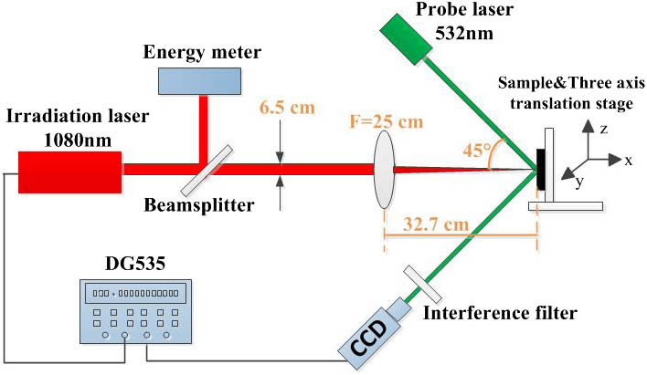
    Fig. 1. Experimental setup for testing damage.
    Real-time images induced by different laser energy densities for (a) 19 and (b) 23 J/cm2, respectively. (c) and (d) Corresponding morphological images taken by an optical microscope (OM) after experiment.
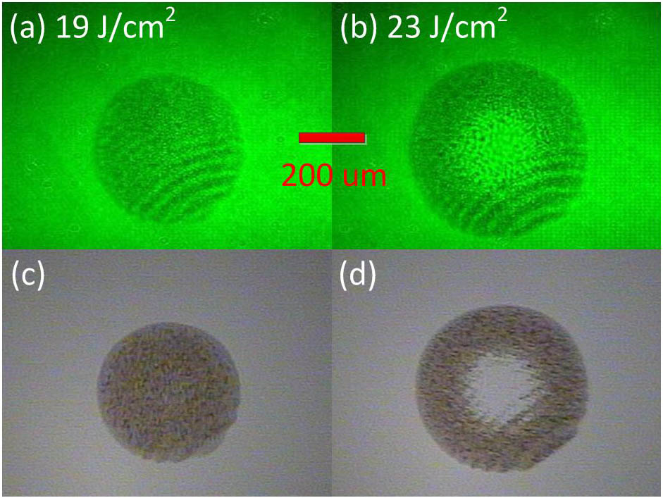
    Fig. 2. Real-time images induced by different laser energy densities for (a) 19 and (b) 23J/cm2, respectively. (c) and (d) Corresponding morphological images taken by an optical microscope (OM) after experiment.
    (a)–(d) Real-time images at different times. The laser energy density is 28 J/cm2. (e) the morphological image taken by the OM after the experiment.
    Fig. 3. (a)–(d) Real-time images at different times. The laser energy density is 28J/cm2. (e) the morphological image taken by the OM after the experiment.
    Simulation model of a silicon wafer under laser irradiation.
    Fig. 4. Simulation model of a silicon wafer under laser irradiation.
    (Color online) (a) Temperature of spot center and (b) von Mises stresses along the X axis at 0.7, 1, 1.1, and 1.3 ms, respectively.
    Fig. 5. (Color online) (a) Temperature of spot center and (b) von Mises stresses along the X axis at 0.7, 1, 1.1, and 1.3 ms, respectively.
    Images just before fracture. The experiment is the same as that of Fig. 3.
    Fig. 6. Images just before fracture. The experiment is the same as that of Fig. 3.
    (Color online) (a) Concentric circle and (b) shear stresses along it at 1.5 ms. S1, S2, and S3 represent the shear stress along (111)[110], (111)[101], and (111)[011], respectively.
    Fig. 7. (Color online) (a) Concentric circle and (b) shear stresses along it at 1.5 ms. S1, S2, and S3 represent the shear stress along (111)[110], (111)[101], and (111)[011], respectively.
    (a) Typical ablation morphology induced by a millisecond laser and (b) a nanosecond laser.
    Fig. 8. (a) Typical ablation morphology induced by a millisecond laser and (b) a nanosecond laser.
    Zhichao Jia, Tingzhong Zhang, Huazhong Zhu, Zewen Li, Zhonghua Shen, Jian Lu, Xiaowu Ni. Stress damage process of silicon wafer under millisecond laser irradiation[J]. Chinese Optics Letters, 2018, 16(1): 011404
    Download Citation