1Ningbo Institute of Materials Technology and Engineering, Chinese Academy of Sciences, Ningbo 315201, China
2University of Chinese Academy of Sciences, Beijing 100049, China
3College of Physics Science & Technology, Laboratory of Optoelectronic Materials and Detection Technology, Guangxi Key Laboratory for the Relativistic Astrophysics, Guangxi University, Nanning 530004, China
4Advanced Micro-Fabrication Equipment Inc., Shanghai 201201, China
5Zhe Jiang Bright Semiconductor Technology Co., Ltd., Jinhua 321026, China
6Advanced Semiconductor Laboratory, King Abdullah University of Science and Technology (KAUST), Thuwal 23955, Saudi Arabia
We report on the carrier dynamic and electronic structure investigations on AlGaN-based deep-ultraviolet multiple quantum wells (MQWs) with lateral polarity domains. The localized potential maximum is predicted near the domain boundaries by first-principle calculation, suggesting carrier localization and efficient radiative recombination. More importantly, lateral band diagrams of the MQWs are proposed based on electron affinities and valance band levels calculated from ultraviolet (UV) photoelectron spectroscopy. The proposed lateral band diagram is further demonstrated by surface potential distribution collected by Kelvin probe microscopy and the density-of-state calculation of energy bands. This work illustrates that lateral polarity structures are playing essential roles in the electronic properties of III-nitride photonic devices and may provide novel perspective in the realization of high-efficiency UV emitters.
1. INTRODUCTION
III-nitride materials have attracted much attention as promising building blocks in optoelectronic and electronic devices, enabling applications including solid-state lighting, DC-AC power conversion, and high-frequency communication, given their wide direct bandgap, high breakdown field, and high thermal conductivity [1–4]. To improve the energy conversion efficiency of the above devices, the analysis of carrier dynamics and electronic structures at the surface and interface plays significant roles. Take a deep-ultraviolet light-emitting diode (DUV-LED) as an example: strong polarization fields in the AlGaN multiple-quantum-well (MQW) active region lead to the separation of electron and hole wave functions and thus result in the quantum-confined Stark effect (QCSE) [5], decreasing internal quantum efficiency (IQE). Additionally, Fermi-level pinning and surface band bending also result in surface states, inhibiting carriers from effectively recombining into photons in quantum-well emitters [6]. Therefore, deeper understanding of the surface/interface properties is strongly desired.
Inversion symmetry is a unique feature of wurtzite III-nitride crystals. The asymmetric nature of the crystal leads to metal polarity and nitrogen polarity of III-nitride thin film with opposite spontaneous polarization fields. These two polarities display noteworthy variations in growth modes and defect incorporation behaviors [7,8], but studies on their surface potentials and band diagrams are very scarce. As reported by numerous researchers, the polarities of III-nitride thin films strongly rely on the underlying low-temperature AlN nucleation layer (NL) prior to the high-temperature (HT) thin-film growth during metal organic chemical vapor deposition (MOCVD) [2,9,10]. On one hand, III polarity is achieved when the HT thin film is grown on a sapphire substrate with AlN NL deposited, whereas N polarity is expected if the growth is carried out directly on sapphire with appropriate nitridation [11,12]. The polarization fields are opposite but the magnitudes are the same for the III- and N-polarity domains. Thus far, virtually all reported III-nitride heterostructures and devices are of single polarity for quality and surface morphology considerations [13,14]. As III- and N-polar domains exhibit properties that are complementary to each other, thin films comprising of both these polarity domains on a single substrate are expected to deliver rich functionalities [12].
MQWs of various polarity surfaces are expected to exhibit significant variation in electronic structure in the case of so-called “lateral-polarity structure” (LPS), where III- and N-polar domains are grown side by side. Kirste et al. previously observed a strong luminescence intensity at the inversion domain boundary (IDB) of GaN thin film [15]. Schuck et al. also reported similar behaviors in GaN with IDBs by means of integrated photoluminescence topography [16]. The enhanced luminescence intensities were ascribed to the maximum of the local potential in the core of the IDB together with two local minima adjacent to the potential maximum, which was first proposed by Fiorentini through ab initio density-functional calculations [17]. Through the utilization of aberration-corrected scanning transmission electron microscopy (STEM), it could analyze the detailed structural features at the IDBs. Both octahedrally and tetrahedrally coordinated metal-nitrogen bonds were demonstrated at the IDBs with sizes of only a few nanometers (nm) [18,19]. However, previous studies on LPS samples are all based on a simple GaN layer. To implement IDBs into optoelectronic devices where an MQW is the active region, the electronic structure and optical properties of both the out-of-plane heterojunctions and the in-plane homojunctions need to be considered. This adds to the complexity of the carrier transportation and recombination processes in the investigated system.
Sign up for Photonics Research TOC. Get the latest issue of Photonics Research delivered right to you!Sign up now
In our previous work, AlGaN/GaN UV MQWs with micrometer-size inversion domains were successfully fabricated [12,20]. We demonstrated that emission intensity of the MQWs with IDBs can be dramatically improved compared to the single-polarity III- and N-polar MQWs. In order to extend the emission wavelength into the DUV region, the Al composition in the AlGaN MQW needs to be larger than 40% [21]. This poses a great challenge on the control of thin-film polarity and interface states because the growth modes are dramatically different between III- and N-polar surfaces [22]. Moreover, the design and optimization of III-nitride optoelectronic devices hinge on device band diagrams to accurately compute and analyze carrier transport and recombination processes [23], although these have not been verified from a theoretical point of view. In the present report, we perform a detailed study on the surface and interface electronic properties of AlGaN DUV-MQWs with IDBs. The lateral band diagram as calculated by the data from ultraviolet photoelectron spectroscopy (UPS) and Kelvin probe microscopy (KFM) can provide in-depth understanding on the carrier transport and recombination mechanism of such novel UV emitters, which is further supported by the theoretical calculation of density of states (DOS).
2 EXPERIMENT
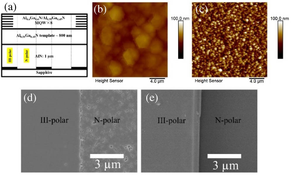
AlGaN/AlGaN DUV MQWs were grown on a 2-inch (50 mm) c-plane sapphire substrate via AMEC Prismo HiT3 MOCVD reactor. Trimethylaluminum, trimethylgallium, and ammonia are used as the Al, Ga, and N sources, respectively. Hydrogen is used as the carrier gas. The fabrication of LPS is based on the patterning of AlN buffers. After deposition of a 20 nm thick LT-AlN buffer on 2 inch (50 mm) sapphire substrate, samples were taken out from the MOCVD chamber, and a standard photolithography patterning process followed by reactive ion etching (RIE) was performed with circular domains ranging from 100 to 500 μm in diameter. Prior to HT thin-film growth, the substrate was subjected to annealing at 1100°C and nitridation at 1050°C. A 1 μm thick AlN layer was grown on the patterned buffers, where polarities were determined by the underlying LT-AlN buffers. Then an 800 nm thick template layer was grown as a transition layer before eight pairs of MQWs deposited on top. The thicknesses of the quantum well (QW) and quantum barrier (QB) are 2.5 nm and 8 nm, respectively. The schematic structures of the MQW sample are shown in Fig. 1(a). The III-polar domains are circular regions with diameters up to 500 μm, located in the N-polar matrix. KOH aqueous solution was used to identify the polarities of the MQW sample. Surface morphologies of the samples were characterized by a Veeco Dimension 3100V atomic force microscope and Hitachi S-4800 field-emission scanning electron microscope (FE-SEM). Crystalline qualities were analyzed using a point-focused high resolution X-ray diffractometer (HRXRD) (Bruker D8 Discover) equipped with a four-bounce symmetric Ge (220) monochromator. Steady-state photoluminescence (PL) studies were performed using a Coherent Ar-F (193 nm) excimer laser at pumping power of , and the luminescence was collected by a Horiba iHR550 spectrometer. The laser spot is around and thus covers both the III- and N-polar domains of the LPS sample. In time-resolved-photoluminescence (TRPL) measurements, samples were excited by a CNI FL-213-Pico 213 nm picosecond diode laser with spot size similar to that of the steady-state PL. The PL decay curves were recorded by a time-correlated single-photon-counting (TCSPC) system. The work functions and electron affinities of the III- and N-polar MQW samples were acquired by UPS measurement, carried out in a Kratos AXIS Ultra-DLD ultrahigh-vacuum photoemission spectroscopy system with an Al α radiation source. Surface potential was further characterized by KFM. Commercial silicon tips with Pt/Ir coating were used as probes.
Figure 1.(a) Schematic structure of AlGaN MQWs with IDBs AFM images of (b) III-polar and (c) N-polar AlGaN MQWs in a μμ region. Top view SEM images of MQWs near IDBs (d) before and (e) after KOH etching.
Theoretical calculations of the surface potentials as well as the DOS in both the III- and N-polar domains and IDBs are performed with the quantum mechanics program Cambridge Serial Total Energy Package (CASTEP), which is based on the first-principle density functional theory (DFT). The valence electronic wave function was expanded in a plane-wave basis vector. All calculations are performed with a plane-wave ultrasoft pseudopotential method combined with the generalized gradient approximation (GGA). The Broyden–Flecher–Goldfarb–Shanno (BFGS) algorithm is used to relax the structure of the crystal models. The convergence precision was set to energy change of below , force of less than 0.01 eV/A, stress of less than 0.02 GPa, and change in displacement of less than in the iterative process. The integral in the Brillouin zone was sampled with the Monkhorst–Pack scheme and special k points of high symmetry. The numbers of k points are . The energy cutoff is 550 eV. All calculations were carried out in reciprocal space with Al: , Ga: , and N: as valence electrons.
3. RESULTS AND DISCUSSIONS
The AFM images of III- and N-polar domains of the MQW samples are shown in Figs. 1(b) and 1(c), respectively. It can be seen that III-polar domains follow a step-flow growth mode, and the surface is covered with hexagons [22,24]. In contrast, in N-polar domains, thin-film growth was initiated through 3D nucleation. The column widths of the 3D crystals are approximately 500 nm, which are slightly larger than those of N-polar AlN as previously reported by Kirste et al. [25]. This can be explained by the fact that the introduction of Ga atoms promotes lateral diffusion and thus leads to larger column sizes [22]. The root-mean-square (rms) roughness of the N-polar domain is 11.5 nm, larger than that of the III-polar domain of AlGaN MQW, which is only 2.1 nm. The crystalline quality of the LPS samples was characterized by HRXRD rocking curves (RCs). The full width at half-maxima (FWHMs) of the (002) and (102) diffraction peaks of the MQWs were measured as 437 and 919 arcsec, respectively, indicating screw type and edge type dislocation densities of and .
To identify the polarities of different domains in the AlGaN MQWs, chemical etching was performed. It is known that the chemical stability of the III-nitride crystal plane is related to its surface energy, which is a function of the dangling bonds density [26]. As the dangling bond density for (000-1) planes is higher than that of (0001) planes, N-polar AlGaN MQWs are more likely to be attacked by ions in alkaline solutions [26,27]. Figures 1(d) and 1(e) clearly show the surface morphologies of AlGaN MQWs near the IDBs before and after 10 min KOH etching. For the MQWs before etching shown in Fig. 1(d), the N-polar domains exhibit a relatively rough surface, whereas the III-polar domains are featureless. The III- and N-polar domains are approximately equal in height. This observation is in accordance with Hoffmann et al., where high Ga composition in the AlGaN with IDBs leads to a large height difference between the two domains due to lateral transport of Ga atoms. However, barely any height difference was observed for high-Al composition AlGaN with IDBs due to the lesser mobility of Al atoms [28]. As shown in Fig. 1(e), the N-polar domains are completely removed after 10 min KOH etching. A sharp interface is clearly observed, exposing the (10-10) crystallographic planes. On the other hand, KOH aqueous solution has no effect on the III-polar domains, as neither etching pits nor hillocks are observed.
The optical properties of the MQWs with IDBs and single uniform III- and N-polarity MQWs were first investigated by steady-state PL measurement. The PL spectra of the MQWs are illustrated in Fig. 2(a). III-polar MQW exhibits a single peak at 280 nm, while N-polar MQW shows a much stronger peak at 310 nm, even though a 280 nm side-emission peak can still be identified. For MQW with IDBs, two peaks located at 280 nm and 310 nm indicate that the emissions are indeed coming from both the III- and N-polar domains. According to Hoffmann et al., Ga atoms are easily diffused across the IDBs, making one polarity domain Ga rich and the other Ga deficient [29]. It has been demonstrated by the same author that peak separations can be obtained in AlGaN epitaxial thin film with two different polarity domains, but the peak position of the N-polar AlGaN was blue-shifted as compared to that of III-polar thin film, which is opposite to our results shown here. This discrepancy suggests that the optical properties of the AlGaN MQWs of different polarities not only depend on the Al composition difference induced by lateral diffusion but also on QW confinement and the geometric scattering effect. It is also noted that luminescence enhancement in the IDB region was not obtained as previously reported by Fiorentini [17] and Kirste et al. [15]. This is induced by the rough surface of the MQWs in the N-polar domains. Carriers will encounter large transporting barriers across the IDBs, proving no advantage in improving the luminescence efficiency of DUV-LEDs over the conventional uniform III-polar samples. The origins of PL peak separation and the techniques to tackle this issue will be shown in a separate work and thus will not be discussed in detail here.
Figure 2.Steady-state (a) PL spectra and (b) PL decay curves of single-polarity MQWs and MQWs with IDBs.
To investigate the carrier dynamics of the AlGaN MQWs with IDBs, TRPL measurements were performed at room temperature (RT). PL decay curves for MQWs with IDBs as well as single-polarity III- and N-polar MQWs are shown in Fig. 2(b) on a logarithmic scale. The hump at about 3 ns for a single III-polarity MQW is the result of the system’s response function (SRF) [30]. The carrier lifetime is obtained by fitting the decay curves over a double-exponential function: and are fast and slow peak intensities before decaying. and are decay lifetimes of the fast and slow components, respectively. The lifetime values are obtained and summarized in Table 1. The lifetime is shortest for III-polar MQW and longest for MQWs with IDBs. Since nonradiative recombination is dominant at RT, the longer decay lifetime achieved for AlGaN MQWs with IDBs suggests a smaller nonradiative recombination rate. This result strongly supports the idea that radiative recombination efficiency is promoted at the IDBs, despite the fact that structural defects such as threading dislocation are usually accompanied by the IDBs [31].
Fast Decay Time (ns)
Slow Decay Time (ns)
Total Decay Time (ns)
III polar
0.08
0.53
0.07
N polar
0.60
2.62
0.49
MQWs with IDBs
0.65
4.46
0.57
Table 1. Calculation of Fast and Slow Components of the Decay Lifetimes
Even though the AlGaN MQW with IDBs shows a smaller nonradiative recombination rate compared to that of single-polarity MQW samples, no direct correlation to the surface potentials has yet been made, which would aid understanding of the unique optical properties of IDB-incorporated UV-MQWs. Through high-resolution TEM, it was found that orientations of III-N bonds are abruptly switched across the IDBs [19]. Fiorentini et al. [17] calculated the local potential in the vicinity of IDBs of the GaN epitaxial layer, and they claimed that the origin of the efficient light emission stems from the potential maximum in the center of the IDBs accomplished by two minima in the N-/III-polar regions using the self-consistent field (SCF) principle after the periodic microscopic oscillations were filtered through a macroscopic average [17]. In this work, first-principle calculations were performed comprehensively near the IDBs of GaN, , and AlN in order to represent the case of an MQW heterostructure. Each of the simulations consists of 32 atoms. The schematic structures and corresponding electronic potentials are shown in Fig. 3. The N-polar domain is located on the left side of the IDBs, whereas the III-polar domain is located on the right. The calculations yield an oscillation of electronic potential at each atom site. The electronic potentials at the IDBs reach the maximum values of , and for GaN, , and AlN, respectively, compared to adjacent atoms. Considering that holes are relatively more localized than electrons due to their heavier masses, hole accumulation is thereby expected at the potential maximum of the IDB region and thus attracts neighboring electrons, leading to a stronger radiative recombination rate.
Figure 3.Schematics of atomic arrangements and corresponding electronic potential distributions near IDBs for (a), (b) GaN; (c), (d) ; and (e), (f) AlN.
As shown in Fig. 4, by inserting an “air gap” laterally into a uniform III-polar GaN and AlN thin film, the free surface of both the III-polar (bottom) and N-polar (top) domains can be created, and their electronic potentials were calculated separately as indicated by the black arrows. Interestingly, the surface potentials are higher for a III-polar surface than those of an N-polar surface by at least 3 eV. In order to support the theoretical calculation, KFM mapping of the AlGaN MQWs in the vicinity of the IDBs was collected and illustrated in Fig. 5(a). Corresponding surface morphology is shown in Fig. 5(b) at the same position. The surface potential of the III-polar domain is indeed higher than that of the N-polar domain, which is in accordance with the theoretical calculation. However, the potential variation is only 150 meV. The smaller potential difference value between the III- and N-polar domains measured from KFM might be due to the carrier screening effect during experiment. Note that surface potential is highly related to the spontaneous polarization of the III-nitride crystals and the background doping concentration. Since KFM measurement was taken in air atmosphere, the polarization bound charges are strongly influenced by the ionized carriers or external charges such as charged gas molecules [6]. The screening charges obviously weaken the surface potential difference. Additionally, unlike the surface potential maximum as predicted by DFT calculation, a smooth transition of the surface potential is observed near the IDBs by KFM. The discrepancy between experiment and theoretical simulation may originate from the rough N-polar surface and rugged interface of the IDB, hindering the lateral carrier flow and efficient recombination. Finally, since the lateral dimension of IDB is only a few nm in an ideal case, much smaller than the lateral diffusion length of Ga and Al atoms of micrometer scale [32], the potential maximum near the IDBs, if any, might not be clearly identified from KFM characterization.
Figure 4.Electronic potential of the free surface of (a) GaN and (b) AlN comprising both [0001] and [000–1] directions.
Figure 5.(a) Surface potential distribution and (b) corresponding topography image of AlGaN MQWs with IDBs in the center. (c) Line-scan of the potential as indicated by the red line in the KFM mapping.
Also note that within III-polar domains, surface potential is the highest along the edges of the AlGaN hexagons as shown in the surface morphologies, while within N-polar domains, the potential contrast is less obvious, especially considering the large roughness of the 3D columns in the N-polar domains. This is strong evidence that surface roughness does not influence the potential distributions by KFM.
The improved optical properties of the AlGaN MQWs with IDBs should be strongly dependent on the band profiles, which accurate computation of carrier transport and recombination processes rely on. Thus, the electronic affinities and valance band levels of III-polar and N-polar AlGaN MQWs were measured by UPS. The valence band (VB) spectra of the samples were examined under monochromatized Al Kα radiation. As shown in Fig. 6, the VB energies below Fermi level are 2.4 and 1.15 eV for N- and III-polar MQWs, respectively, suggesting a much larger upward band bending at the surface of III-polar domains than that in N-polar domains. This result agrees with earlier reports on III- and N-polar GaN thin films, where an upward band bending at the surface of Ga-polar GaN and a downward band bending at the surface of N-polar GaN were observed [6,33]. The cutoff energies of the AlGaN MQWs are 10.6 and 11.29 eV for N- and III-polar MQWs, respectively. Thus, the electron affinity (EA) can be determined by Eq. (2): where is the energy of the incident photons of 21.22 eV, msub is the spectral width, and is the bandgap of the top layer (4.64 eV). Electron affinities are calculated to be 8.39 and 6.44 eV for N- and III-polar AlGaN MQWs, respectively.
Figure 6.VB spectra and cutoff values measured from N- and III-polar AlGaN MQWs via UPS.
Based upon the electron affinities and valence band edges calculated from Fig. 6, a lateral band diagram of AlGaN MQWs in the vicinity of IDBs is illustrated in Fig. 7. A lateral built-in potential of 1.25 eV is obtained, promoting lateral electron diffusion from III-polar to adjacent N-polar domains. Additionally, the Fermi levels relative to the vacuum level—in other words, the work function of semiconductors —can also be extracted from the lateral band diagram. As clearly illustrated, the work function of III-polar AlGaN MQW is 0.7 eV lower compared to that of N-polar AlGaN MQW, suggesting that the surface potential of III-polar AlGaN MQW should be higher than that of an N-polar surface, since the relative difference between the work functions of the KFM tip and semiconductor () is directly related to the surface potential difference (). This is exactly what KFM has shown before in Fig. 5. The proposed lateral band diagram is herein further confirmed by the results obtained. It is worth mentioning that the band offset between III- and N-polar domains of the LPS-MQWs originates from different Fermi levels of the adjacent domains instead of the polarization effect. The band diagram shown in Fig. 7 is illustrated by an “in-plane” configuration, where no spontaneous and piezoelectric fields are present.
Figure 7.Lateral band diagram of AlGaN MQWs with IDBs located in the center.
Finally, in order to examine the band bending in MQWs with IDBs, a model of AlN thin film with IDBs is built and calculated by CASTEP. The surface dangling bonds of the AlN model are saturated by a number of H atoms. The DOS distribution is drawn from the third layer of atoms away from the surface, and thus the influence from the very top surface is negligible. The DOS distribution of the conduction band and valence band across the IDB structure is shown in Fig. 8. The lateral position corresponds to the above atom location in AlN thin film with IDB. From the DOS distribution across the IDB, the valence band shows large downward bending from the Al-polar domain to the N-polar domain exceeding 1 eV. This is in perfect agreement with our proposed lateral band diagram. The DOS of the conduction band is relatively low, considering the large bandgap of AlN, and thus there is a lower density of electrons in the conduction band. The slight higher DOS of the conduction band in the N-polar domain is consistent with the higher background carrier concentration in N-polar domains and is in line with the higher luminescence intensity of the LPS. In fact, a combination effect of the unique lateral band structure, surface scattering effect, and higher DOS in the N-polar domain will benefit the efficient carrier recombination in LPS-MQWs.
Figure 8.DOS calculation of AlN with IDBs in the center. The left side indicates III polarity, and the right side indicates N polarity.
In all, on the basis of the lateral band diagram, we can postulate that higher luminescence intensities in the AlGaN MQWs with IDBs come from the carrier recombination not only vertically but also laterally, and thus create a three-dimensional carrier recombination pathway. To the best of our knowledge, this work is the first demonstration of the lateral band diagram in AlGaN-MQWs with IDBs. Although the performance of DUV-LEDs is not yet as good as their visible-wavelength counterparts, it is possible that introduction of IDBs into MQWs may provide another perspective in the design of MQWs and lay a solid foundation for the development of next-generation UV emitters.
4. CONCLUSION
By introducing lateral polarity domains into AlGaN DUV-MQWs, unique optical properties and enhanced radiative recombination rate were demonstrated for AlGaN MQWs with lateral polarity domains compared to conventional single-polarity MQW structure. A potential maximum was calculated near the domain boundary via DFT, where hole accumulation could join the efficient radiative recombination, even though a smooth potential transition is observed at the domain boundaries experimentally due to limitation of space resolution. Based on a combined data analysis of UPS and KFM, the lateral band diagram of AlGaN MQWs is proposed for the first time. The band diagram was further validated by the calculation of DOS distribution of the conduction and valence bands in the lateral direction. Our work provides an unambiguous demonstration of the carrier dynamic process and electronic structure in AlGaN MQWs with both III- and N-polar surfaces. These understandings enable rational design of future DUV emitters for improved performance.