
Shuangyi Zhao, Qionghua Mo, Wensi Cai, Huaxin Wang, Zhigang Zang. Inorganic lead-free cesium copper chlorine nanocrystal for highly efficient and stable warm white light-emitting diodes[J]. Photonics Research, 2021, 9(2): 187
- Photonics Research
- Vol. 9, Issue 2, 187 (2021)
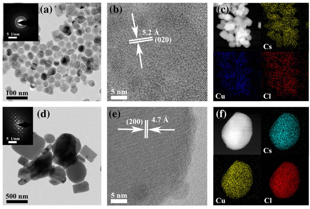
Fig. 1. (a) Transmission electron microscopy (TEM), (b) high-resolution TEM (HRTEM) images, and (c) corresponding cesium (Cs), copper (Cu), and chlorine (Cl) elemental mapping images of Cs 3 Cu 2 Cl 5 CsCu 2 Cl 3
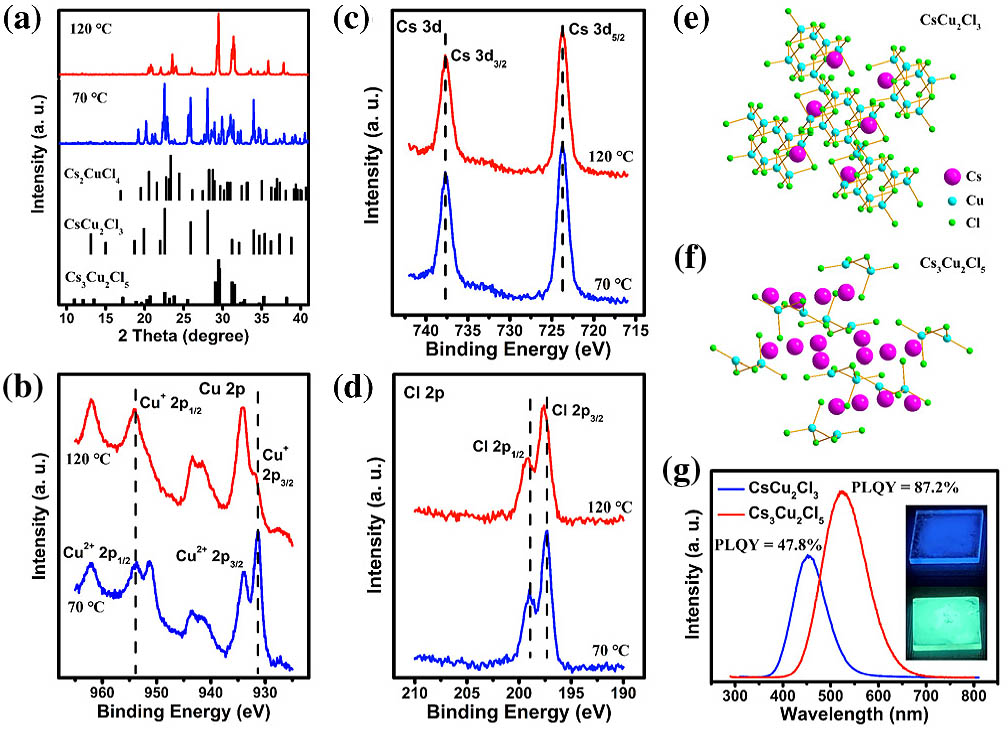
Fig. 2. (a) XRD patterns of the cesium copper chlorine colloidal perovskite synthesized at 70°C and 120°C, as well as the standard XRD patterns. High-resolution X-ray photoelectron spectroscopy (XPS) spectrum of (b) Cu 2p, (c) Cs 3d, (d) Cl 2p. (e), (f) Crystal structure of 3D CsCu 2 Cl 3 Cs 3 Cu 2 Cl 5 CsCu 2 Cl 3 Cs 3 Cu 2 Cl 5 CsCu 2 Cl 3 Cs 3 Cu 2 Cl 5
Fig. 3. Photoluminescence exciton (PLE) spectra of (a) CsCu 2 Cl 3 Cs 3 Cu 2 Cl 5 Cs 3 Cu 2 Cl 5 CsCu 2 Cl 3 CsCu 2 Cl 3 Cs 3 Cu 2 Cl 5
Fig. 4. (a), (c) Luminescent spectrum and (b), (d) CIE chromaticity diagram of CsCu 2 Cl 3 Cs 3 Cu 2 Cl 5
Fig. 5. (a) EL spectra of as-fabricated white light-emitting diodes (WLEDs). The insets are the photographs of the emissive WLEDs obtained in the daylight (left) and dark (right). (b) CIE chromaticity diagram of the WLEDs. (c) Pseudocolor plot of the EL spectra of long-time operating WLEDs. (d) Evolution of the normalized luminous efficiency (LE) and CRI values as functions of operating time. (e) CCT of the WLED as a function of the operating time in atmosphere.

Set citation alerts for the article
Please enter your email address
© Copyright 2018-2021 | Chinese Laser Press. All Rights Reserved 沪ICP备15018463号-20