• Photonics Research
  • Vol. 11, Issue 9, 1583 (2023)
Gangyi Zhu1、*, Xin Ji1, Zhenfu Zhang2, Xingcan Yan1, Ying Yang1, Feifei Qin1, Xin Li1, Jiagui Wu3, Xiaojuan Sun4, Junbo Yang2、5, and Yongjin Wang1
Author Affiliations
  • 1GaN Optoelectronic Integration International Cooperation Joint Laboratory of Jiangsu Province, Nanjing University of Posts and Telecommunications, Nanjing 210003, China
  • 2College of Arts & Science, National University of Defense Technology, Changsha 410003, China
  • 3School of Physical Science and Technology, Southwest University, Chongqing 400715, China
  • 4State Key Laboratory of Luminescence and Applications, Changchun Institute of Optics, Fine Mechanics and Physics, Chinese Academy of Sciences, Changchun 130033, China
  • 5e-mail: yangjunbo@nudt.edu.cn
  • show less
    DOI: 10.1364/PRJ.490145 Cite this Article Set citation alerts
    Gangyi Zhu, Xin Ji, Zhenfu Zhang, Xingcan Yan, Ying Yang, Feifei Qin, Xin Li, Jiagui Wu, Xiaojuan Sun, Junbo Yang, Yongjin Wang. Electrically pumped optomechanical beam GaN-LED accelerometer based on the quantum-confined Stark effect[J]. Photonics Research, 2023, 11(9): 1583 Copy Citation Text show less

    Abstract

    Micro-nano optomechanical accelerometers are widely used in automobile, aerospace, and other industrial applications. Here, we fabricate mechanical sensing components based on an electrically pumped GaN light-emitting diode (LED) with a beam structure. The relationship between the blueshift of the electroluminescence (EL) spectra and the deformation of the GaN beam structure based on the quantum-confined Stark effect (QCSE) of the InGaN quantum well (QW) structure is studied by introducing an extra mass block. Under the equivalent acceleration condition, in addition to the elastic deformation of GaN-LED, a direct relationship exists between the LED’s spectral shift and the acceleration’s magnitude. The extra mass block (gravitational force: 7.55×10⁻¹¹ N) induced blueshift of the EL spectra is obtained and shows driven current dependency. A polymer sphere (PS; gravitational force: 3.427×10⁻¹² N) is placed at the center of the beam GaN-LED, and a blueshift of 0.061 nm is observed in the EL spectrum under the injection current of 0.5 mA. The maximum sensitivity of the acceleration is measured to be 0.02 m/s2, and the maximum measurable acceleration is calculated to be 1.8×10⁶ m/s2. It indicates the simultaneous realization of high sensitivity and a broad acceleration measurement range. This work is significant for several applications, including light force measurement and inertial navigation systems with high integration ability.

    1. INTRODUCTION

    Acceleration sensors are widely used in aerospace [1], vibration sensing [2,3], and the automobile industry [4,5]. In particular, a large number of acceleration sensors based on microelectromechanical systems (MEMS) or micro-optical-mechanical systems (MOEMS) have been reported, which can be realized by capacitive [6,7], piezoelectric [8], the tunneling effect [9,10], resonant [11], or optomechanical methods [1214]. Compared with the MEMS structure, optomechanical accelerometers have advantages of small size, high sensitivity, extensive measurement range, low cost, high reliability, low power consumption, and batch manufacturing. It has become a research hotspot in recent years. According to the optomechanical measurement principle, the displacement of mass caused by acceleration leads to optical phenomena such as interference and diffraction, which can be used to measure acceleration. Normally, the optical accelerometer has a higher sensitivity and resolution than the MEMS acceleration sensor. An optomechanical accelerometer designed to search for vector dark matter has been reported to have the best accuracy [3]. Most commercial optomechanical accelerometers are based on Si materials. However, indirect bandgap, low mechanical strength, and low piezoelectric coefficients of Si materials hinder the further development of silicon-based acceleration with high sensitivity and an extensive measurement range.

    As a third-generation semiconductor material, GaN has excellent mechanical, photoelectric, optical, piezoelectric, thermal, chemical, and biochemical properties, which makes it suitable for application under high temperatures and corrosive environments [1517]. GaN with a high Young’s modulus and yield stress can obtain a linear relationship between the applied load and induced deformation [18]. Therefore, GaN is a promising material for fabricating optical [19,20] and MEMS devices [21,22] in harsh environments. However, only some reported devices could have comprehensively considered the GaN characteristics. A single light source, power, or MEMS device has been prepared based on a single characteristic. Some researchers have tried to combine the optical and mechanical properties of GaN to prepare stress sensors. Dong et al. [23] and Peng et al. [24] fabricated stress sensors based on GaN nanowires by graphically epitaxial lift-off (GELO) and microfabrication, respectively. The relationship between photoluminescence (PL) and stress is systematically studied, suggesting that the blueshift or redshift of spectra originated from the quantum-confined Stark effect (QCSE) phenomenon [25]. Please take advantage of GaN’s feature in micromachining. Highly integrated devices can be designed. However, these GaN stress sensors need a laser as an external excitation source, which may limit their high-density chip integration density and further applications.

    In this study, we comprehensively take advantage of the mechanical, optical, and electrical properties of GaN materials to design and fabricate an electrically pumped GaN light-emitting diode (LED) with a beam structure. GaN-LED with beam structure here can be used as a light component and mechanical sensing component. Through introducing an extra mass block, the relationship between the blueshift of the electroluminescence (EL) spectra and the deformation of GaN beam structure based on the QCSE of InGaN quantum well (QW) structure was studied. Under the equivalent acceleration condition, the deformation-induced spectral shift is directly related to the acceleration magnitude. The PS sphere estimates the maximum sensitivity and measurable region, which can be calculated via simulation. The fabricated beam GaN-LED accelerometer can simultaneously realize high sensitivity (0.02  m/s2) and broad measurement range (1.8×10⁶  m/s2) of acceleration. Therefore, we believe the proposed acceleration sensor is significant for several applications, such as developing multipurpose devices and inertial navigation systems with high integration ability.

    2. EXPERIMENTAL SECTION

    A. Fabrication of GaN Beam Accelerometer

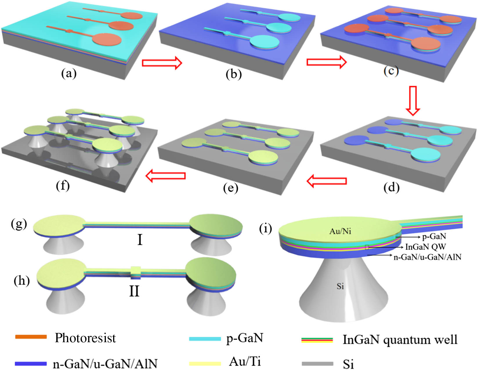
    To make the uniformity of the devices, electrically pumped beam GaN-LED accelerometers are fabricated based on the commercial InGaN QW epitaxial layer on a silicon substrate via semiconductor micro-nano processing technology. The GaN epitaxial layer from bottom to top consists of a 2.1-μm-thick undoped AlN and GaN layer (u-GaN), 1.5-μm-thick n-GaN layer, 1.3-μm-thick AlGaN layer, 50-nm-thick GaN/InGaN QW multi-layer, and 0.55-μm-thick p-GaN layer. The fabrication process of the GaN-LED accelerometer with beam structure is illustrated in Figs. 1(a)–1(f). First, the structures of type I and II devices are patterned on the photoresist layer by photolithography (step a). An epitaxial layer with a thickness of 2.5 μm is etched to the n-GaN layer by inductively coupled plasma reactive ion etching (ICP RIE) with a photoresist layer as a mask. Then, the residual photoresist is removed using an acetone solution (step b). The accelerometer beam pattern is defined by photolithography again (step c), followed by ICP etching with a thickness of about 3.0 μm to the silicon substrate layer and removing the residual photoresist (step d). Second, the photoresist layer is again patterned by photolithography. The p-electrode and n-electrode are prepared on the n-GaN and p-GaN layers by electron beam evaporation and removing residual photoresist with an acetone solution. The electrode material comprises 20 nm nickel and 100 nm gold (step e). Finally, the GaN beam is etched by HNF solution (HF:HNO3=1:1) via isotropic wet etching to suspend the beam from the silicon layer. The silicon substrate under the disk is etched into columns to support the beam accelerometer devices (step f). GaN LEDs with type I [Fig. 1(g)] and type II [Fig. 1(h)] beam cavities are obtained. The material details for the cavity at the beam position are shown in Fig. 1(i). It comprises surface electrodes, p-GaN, QW, n-GaN, and the buffer and Si substrate layers.

    Fabrication process of GaN-LED accelerometer with beam structure: (a) patterning the photoresist, (b) etching to the n-GaN layer, (c) patterning the photoresist layer again, (d) etching to the Si substrate layer, (e) patterning the photoresist layer and preparing electrode, and (f) wet isotropic etching of silicon. Schematics of beam GaN-LED accelerometers with two structures: (g) type I, (h) type II. (i) Cross-sectional image for part of the GaN beam devices.

    Figure 1.Fabrication process of GaN-LED accelerometer with beam structure: (a) patterning the photoresist, (b) etching to the n-GaN layer, (c) patterning the photoresist layer again, (d) etching to the Si substrate layer, (e) patterning the photoresist layer and preparing electrode, and (f) wet isotropic etching of silicon. Schematics of beam GaN-LED accelerometers with two structures: (g) type I, (h) type II. (i) Cross-sectional image for part of the GaN beam devices.

    B. Device Characterization

    Scanning electron microscopy (SEM; Hitachi SU-8010) is used to characterize the structure of the beam accelerometers. A high-resolution spectrometer (Ocean Optics HR4000) acquires the EL spectra of devices under free space. The current–voltage (I–V) and capacitance-voltage (C–V) characteristics of devices are obtained by a semiconductor device analyzer (Agilent Technologies B1500A). All these measurements are conducted at room temperature.

    3. RESULTS AND DISCUSSION

    A. Device Designation

    Two types of devices are designed to demonstrate the accelerometer properties. The type I accelerometer (Fig. 1) has a beam structure, and the type II accelerometer [Fig. 1(h)] has a beam structure with a sensitive mass block in the center of the beam. These two types of devices can be fabricated with the standard semiconductor process. Compared with the type I accelerometer, the deformation degree of the type II accelerometer can be higher by orders of magnitude under the same acceleration. Thus, the type II accelerometer can amplify the influence of acceleration to be measured on the variation in the optical signal.

    B. Electrical and EL Properties of Two Types of Accelerometer

    The SEM images of GaN-LED accelerometers with beam structure are shown in Fig. 2. Figures 2(a) and 2(b) show the top and side views of the type I device. The beam structure’s length, width, and thickness are 300, 16, and 5.5 μm, respectively. The density of GaN material is 6.1  g/cm3, so the beam mass of the type I accelerometer is calculated to be 1.61040×10⁷  g. The diameter of the microdisk is 150 μm. The prepared device has good surface quality. From the side view, it can be seen that the beam structure is wholly suspended. Due to the removal of the silicon substrate, the fabricated accelerometer beam structure can decrease the optical loss of the beam in the vertical direction and improves the light confinement effect, which facilitates high-performance light emission [26,27]. The beam structure can also serve as an optomechanical component and elastic deformation is generated by acceleration. Figures 2(c) and 2(d) show the top and side views of type II devices. Figure 2(e) displays the enlarged SEM image of the extra mass block. Compared with the type I device, the extra mass block is made of two symmetric trapezoids with a top base of 13.5 μm, bottom base of 24.8 μm, height of 6 μm, and thickness of 5.5 μm. The volume and mass of the extra mass block are 1.2639×10⁹  cm3 and 7.70979×10⁹  g, respectively. According to Newton’s second law of motion, F=ma, the extra mass block is equivalent to a confident acceleration. For type I structure, the mass of the extra mass block is 7.70979×10⁹  g, which corresponds to a gravitational force of 7.55×10¹¹  N, i.e., an equivalent acceleration of 0.47  m/s2.

    SEM images of GaN-LED accelerometer with beam structure. (a) Top view of type I device; (b) side view of type I device; (c) top view of type II device; (d) side view of type II device; (e) enlarged image of the top view of sensitive mass block; (f) array of type II device.

    Figure 2.SEM images of GaN-LED accelerometer with beam structure. (a) Top view of type I device; (b) side view of type I device; (c) top view of type II device; (d) side view of type II device; (e) enlarged image of the top view of sensitive mass block; (f) array of type II device.

    Figures 3(a) and 3(b) display the luminous images of the two devices at an injection current of 0.5 mA. Due to the particular electrode structure, current will be injected from the right p-layer to the left n-layer from the beam. Since the beam cavity is long, carrier combination more easily happens in the concentrated region. Unlike the surface electrode state, emission occurs at the beam end for type I devices and at the center for type II devices. Figures 3(c) and 3(e) show the EL spectra of the two devices at different injection currents. With the increase in the injection current, the emission intensity of the beam GaN-LED accelerometers also increases. Both devices have a small full width at half-maximum (FWHM). This is because the beam structure reduces the optical loss in the vertical direction and confines the light in the microcavity, which is conducive to improving the EL properties of beam devices. Figure 3(d) displays the EL intensity of the two devices at different injection currents. For an LED, EL properties such as the intensity FWHM are related to the injection current, cavity temperature, cavity structures, etc. As shown in Fig. 3(d), the EL intensity of the two devices increases with the increase in the injection current. Under the same current, the emission intensity of the type II accelerometer is greater than that of the type I device. The above phenomenon may be attributed to two reasons. First, the type II device has a larger luminous area than the type I device, and it has a higher ratio of area to circumference and, therefore, emits light more efficiently. Second, the luminous efficiency of type II devices is higher than that of type I devices because the inner stress of the epitaxial layer suppresses the exciton–exciton annihilation in InGaN QW [28]. Third, the difference in junction area may also influence the EL intensity. The injected electrical power converts into heat in two significant ways: the nonradioactive recombination from the active region and the joule heat from the p-type layers. For the same current, the voltage of the type I device is higher than the type II device [Fig. 4(a)], so joule heat is higher in the type I device. In this case, EL intensity will be decreased.

    Luminous images of the beams: (a) type I accelerometer, (b) type II accelerometer. EL spectra of the two types of beam GaN-LED accelerometers measured at different injection currents: (c) type I accelerometer, (e) type II accelerometer. (d) The emission intensity of two types of accelerometers at different injection currents. (f) The full width at half-maximum (FWHM) of the two types of beam GaN-LED accelerometers at different injection currents.

    Figure 3.Luminous images of the beams: (a) type I accelerometer, (b) type II accelerometer. EL spectra of the two types of beam GaN-LED accelerometers measured at different injection currents: (c) type I accelerometer, (e) type II accelerometer. (d) The emission intensity of two types of accelerometers at different injection currents. (f) The full width at half-maximum (FWHM) of the two types of beam GaN-LED accelerometers at different injection currents.

    (a) I–V curves of the two types of beam GaN-LED accelerometers. The inset shows the data in logscale. (b) C–V curves of two types of accelerometers at a frequency of 100 kHz. (c) Relationship between the peak EL wavelength and injection current for the two types of GaN-LED accelerometers; the inset displays a schematic of the InGaN QW’s polarization direction, (d) beam displacement of the two types of GaN-LED accelerometers under standard gravity field obtained using COMSOL simulation.

    Figure 4.(a) IV curves of the two types of beam GaN-LED accelerometers. The inset shows the data in logscale. (b) CV curves of two types of accelerometers at a frequency of 100 kHz. (c) Relationship between the peak EL wavelength and injection current for the two types of GaN-LED accelerometers; the inset displays a schematic of the InGaN QW’s polarization direction, (d) beam displacement of the two types of GaN-LED accelerometers under standard gravity field obtained using COMSOL simulation.

    Figure 3(f) shows the FWHM of the two devices at different injection currents. The FWHM of the two GaN-LED accelerometer types increases with the current injection increase. When the injection current is increased from 0.4 to 1.0 mA, the FWHM of the type I accelerometer is in the range of 16–18 nm, while that of the type II accelerometer ranges from 13 to 14 nm. As the current injection increases, the FWHM of both devices also increases. The changes in FWHM may be ascribed to the internal quantum efficiency (IQE) droop [29] or the increase of carrier density (N) and the temperature (T) in QWs. Changing N and T may result in variation of carrier distribution in the allowed bands, and all result in increasing FWHM. Further, the FWHM of type II devices is more minor than type I devices. This indicates that the cavity efficiency of the type II device is greater than that of the type I device due to the extra mass block.

    Figure 4(a) displays the IV curves for the two types of beam GaN-LED accelerometers. The turn-on voltages of type I and type II devices are approximately 3.5 and 3 V, respectively. The turn-on voltage of a type II device is smaller than that of a type I device due to the larger electrode area of a type II device. Besides, the IV curve in logscale inserted in Fig. 4(a) also indicates a heave leakage current. This phenomenon can be correlated to shunt resistance, which depends on the defect level in the LED structure. For smaller voltages, the difference could be just local defect density, increasing tunneling current for devices of type II. Due to the large area, the surface damage induced by the ICP etching or fabrication of surface electrodes is heavy. Judging from these results, the turn-on voltage of the LEDs will be high. Figure 4(b) shows the CV curves for the two types of accelerometers at a frequency of 100 kHz. The capacitance of the two types of accelerometers first increases and then decreases in the bias voltage range of 4 to 4 V. Finally, the negative capacitance (NC) phenomenon is observed [30,31]. The capacitance of the pn junction under forward bias includes depletion layer capacitance and diffusion capacitance. Before the turn-on voltage is reached, the junction capacitance mainly comprises depletion layer capacitance. The maximum capacitance values of type II and I devices are 19 and 18 pF at the voltage above 3 V, respectively. The difference between the two capacitances can be attributed to the larger area of type II devices than that of type I devices. When the voltage reaches the turn-on voltage, the diffusion capacitance rapidly increases, and then the junction capacitance is mainly composed of diffusion capacitance. The capacitance of the two types of devices rapidly decreases, and the capacitance of the type II device becomes smaller than that of the type I device. Type II device has a more robust NC behavior than type I device. This can be ascribed to the fact that the radiation recombination efficiency of carriers in the active region of type II devices is higher than that of type I due to the larger electrode area [32]. Figure 4(c) displays the relationship between peak EL wavelength and injection currents for the two types of devices. The EL spectra show two distinct characteristics. First, an obvious blueshift is observed in the two types of GaN-LED accelerometers with the increase in the injection current. Second, the spectral blueshift magnitude of the type II device is more significant than that of the type I device at the same injection current.

    The blueshift of GaN EL spectra can be attributed to the weakening of QCSE [3335] induced by the spontaneous polarization Psp and piezoelectric polarization Ppz of InGaN QW. The direction of spontaneous polarization is downward, while that of piezoelectric polarization is upward, as illustrated in the inset of Fig. 4(c). For optomechanical GaN-LED with beam structure, a specific gravitational force is applied to the beam. Thus, the top surface of the beam is compressed in the horizontal direction, while the InGaN QW layer on the top surface of the beam is stretched in the vertical direction due to the Poisson effect [36,37]. The piezoelectric polarization increases, and the total polarization decreases, which leads to the remission of total polarization induced by QCSE. The first characteristic, i.e., an obvious blueshift is observed in both types of GaN-LED accelerometers with the increase in the injection current, can be attributed to the screening effect of the QCSE by the injected carriers. The second characteristic is that the magnitude of the blueshift of the type II device is more significant than that of the type I device at the same injection current. This can be ascribed to the fact that the deformation or displacement of a type II device is more significant than that of a type I device under a particular gravity field. According to the geometric parameters of the fabricated device, the beam GaN-LED accelerometer models are established by COMSOL software. The mechanical parameters of GaN material used in the model are as follows: shear modulus at (001) plane=116  GPa, Young’s modulus=287  GPa, and yield stress=200  MPa [3842]. When we look at beam 143 μm from the side, the displacements of type II and type I devices in the Z direction are 2.88 and 3.03 pm, respectively, as illustrated in Fig. 4(d).

    As can be seen in Fig. 2(c), there is an extra mass in the center of the type II accelerometer compared to the type I accelerometer. Since the GaN beam is suspended, the gravity of the extra mass block will cause the sharp changes of the device and blueshift the central wavelength of EL via QCSE. Based on this phenomenon, one can fabricate an accelerometer. Taking the data at 0.5 mA as an example, the weight of this extra mass block is 7.70979×10⁹  g, which corresponds to a gravitational force of 7.55×10¹¹  N, i.e., an equivalent acceleration of 0.47  m/s2. If the acceleration can be measured by characterizing the blueshift of the EL spectral peak, the blueshift of the EL spectral peak is 4.6 nm at an injection current of 0.5 mA. Therefore, the electrically pumped, optomechanical GaN-LED with beam structure can be used as a high-performance accelerometer.

    C. Maximum Measurable Range’s Simulation of Type II Accelerometer

    Two issues, which are the wavelength shift of EL and the sharp changes of the GaN beam, can determine the performance of the accelerometer. The EL spectra of the GaN LED can be measured conveniently; thus, the maximum measurable region of the GaN accelerometer mainly lies on the mechanical characteristics of the cavity. To figure it out, the mechanical properties of type II GaN-LED accelerometers are analyzed by finite element simulation. Based on this simulation model, the inner stress distribution of the beam GaN-LED device is shown in Fig. 5. The maximum stress of the device appears on the left side. The enlarged structure is shown in Fig. 5(b), where the color bar indicates that the maximum stress reaches 200 MPa at the fracture point of GaN material. The corresponding maximum acceleration is calculated as 1.8×10⁶  m/s2 by COMSOL simulation. Thus, the maximum measurable acceleration of a type II accelerometer device can be considered as 1.8×10⁶  m/s2. Figure 5(c) shows the beam’s vertical deformation occurring near the center’s left side under an acceleration of 1.8×10⁶  m/s2. The maximum displacement is approximately 0.55 μm in the vertical direction. Figure 5(d) shows the transverse displacement of the beam. The maximum transverse displacement of 3.2 nm appears at the step structure, which is also the most vulnerable to fracture.

    (a) Beam stress distribution of beam GaN-LED device; (b) enlarged stress distribution of the device. (c) Vertical (Z axis) displacement and (d) horizontal (Y axis) displacement of the device. The acceleration is 1.8×10⁶ m/s2.

    Figure 5.(a) Beam stress distribution of beam GaN-LED device; (b) enlarged stress distribution of the device. (c) Vertical (Z axis) displacement and (d) horizontal (Y axis) displacement of the device. The acceleration is 1.8×10⁶  m/s2.

    D. Minimum Sensitivity of Type II Accelerometer

    Based on the simulation in Fig. 5, the shape changes are various; thus, the minimum sensitivity of type II accelerometer is mainly related to the EL shift. Among the two types of beam GaN-LED accelerometers, the type II device has better acceleration sensitivity due to the sensitive mass block. To measure the minimum sensitivity of a type II device, a polymer sphere (PS) is placed at the center of the beam of a device by spin-coating PS solution, as shown in Figs. 6(a) and 6(b). The diameter of PS (material density: 1.05  g/cm3) is nearly 8.6 μm, as shown in Fig. 6(c), and the mass of PS is 3.4969×10¹⁰  g, corresponding to a gravitational force of 3.427×10¹²  N. As illustrated in Fig. 7(d), the corresponding Z direction displacement, in this case, is obtained at 0.02 pm by COMSOL simulation. It indicates that the PS can change the sharpness of the GaN beam slightly. With the equation F=ma, the calculated acceleration is 0.02  m/s2.

    SEM images of type II device with PS. (a) Top view, (b) side view. (c) Enlarged image of beam structure with PS.

    Figure 6.SEM images of type II device with PS. (a) Top view, (b) side view. (c) Enlarged image of beam structure with PS.

    (a) EL spectra of the type II device after adding PS at different injection currents. (b) I–V curves of type II device before and after adding PS; the inset image displays the illumination of the beam structure. (c) Relationship between peak wavelength of EL spectra and injection current before and after adding the PS. (d) Displacement of the beam before and after adding PS under standard gravity field.

    Figure 7.(a) EL spectra of the type II device after adding PS at different injection currents. (b) IV curves of type II device before and after adding PS; the inset image displays the illumination of the beam structure. (c) Relationship between peak wavelength of EL spectra and injection current before and after adding the PS. (d) Displacement of the beam before and after adding PS under standard gravity field.

    The EL spectra of type II devices with PS are shown in Fig. 7(a). Evident light emission from the beam structure is observed in Fig. 7(b) inset image. After adding PS, the IV curve of the type II device indicates good rectification characteristics with a turn-on voltage of 3 V in Fig. 7(b). The turn-on voltage of the type II device after adding PS becomes slightly higher than before adding PS, and it is because of the passivation of the sidewalls caused by the application of the solution containing PS. The IV characteristics verify the application of a type II device as an accelerometer. A blueshift of 0.061 nm is observed in the EL spectrum at the peak wavelength after adding PS under an injection current of 0.5 mA. The blueshift reaches the spectral resolution limit of the spectrometer, as illustrated in Fig. 7(c). Interestingly, the peak wavelength of the device without or with PS is different with the increasing current. It is +0.061  nm for 0.5 mA and around 0.05nm for 0.9 mA. Blueshift of the peak wavelength is due to the quantum domain limited Steinke effect, and it is related to the PS-induced shape change of the GaN beam and the driving current. Since the displacement of the beam is minimal (0.02 pm), the blueshift will be unobvious for high currents. The minimum acceleration sensitivity of the type II accelerometer device can be considered as 0.02  m/s2.

    4. CONCLUSION

    To summarize, we comprehensively took advantage of the mechanical, optical, and electrical properties of GaN material to prepare a novel electrically pumped, optomechanical GaN-LED accelerometer with a beam structure. Extra mass block induced blueshift of EL spectra was obtained based on the weakening of the QCSE, and it shows driven current dependency. Under equivalent acceleration, along with the elastic deformation of GaN-LED, a direct relationship was observed between the blueshift of EL spectra and the acceleration magnitude. The maximum sensitivity of the acceleration is measured to be 0.02  m/s2, and the maximum measurable acceleration is calculated to be 1.8×10⁶  m/s2, which indicates that the fabricated accelerometer could realize high sensitivity and broad acceleration measurement range in harsh environments. This facilitates a method to measure pN-level force by testing the peak shift of the EL spectrum in the future. This work is significant for developing one multipurpose device for inertial navigation systems.

    Acknowledgment

    Acknowledgment. We thank Professor X. Wang at Ningbo University for his discussion and Dr. X. X. Wang at Southeast University for her help with the artwork.

    References

    [1] F. Liu, S. Alaie, Z. C. Leseman, M. Hossein-Zadeh. Sub-pg mass sensing and measurement with an optomechanical oscillator. Opt. Express, 21, 19555-19567(2013).

    [2] F. Zhou, Y. Bao, R. Madugani, D. A. Long, J. J. Gorman, T. W. LeBrun. Broadband thermomechanically limited sensing with an optomechanical accelerometer. Optica, 8, 350-356(2021).

    [3] J. Manley, M. Chowdhury, D. Grin, S. Singh, D. J. Wilson. Searching for vector dark matter with an optomechanical accelerometer. Phys. Rev. Lett., 126, 061301(2021).

    [4] X. Zou, P. Thiruvenkatanathan, A. A. Seshia. A seismic-grade resonant MEMS accelerometer. J. Microelectromech. Syst., 23, 768-770(2014).

    [5] R. Middlemiss, A. Samarelli, D. Paul, J. Hough, S. Rowan, G. Hammond. Measurement of the earth tides with a MEMS gravimeter. Nature, 531, 614-617(2016).

    [6] C. Acar, A. M. Shkel. Experimental evaluation and comparative analysis of commercial variable-capacitance MEMS accelerometers. J. Micromech. Microeng., 13, 634-645(2003).

    [7] H. Kulah, J. Chae, N. Yazdi, K. Najafi. Noise analysis and characterization of a sigma-delta capacitive microaccelerometer. IEEE J. Solid-State Circ., 41, 352-361(2006).

    [8] S. Tadigadapa, K. Mateti. Piezoelectric MEMS sensors: state-of-the-art and perspectives. Meas. Sci. Technol., 20, 092001(2009).

    [9] C. H. Liu, A. M. Barzilai, J. K. Reynolds, A. Partridge, T. W. Kenny, J. D. Grade, H. K. Rockstad. Characterization of a high-sensitivity micromachined tunneling accelerometer with micro-g resolution. J. Microelectromech. Syst., 7, 235-244(2009).

    [10] H. Nakstad, J. T. Kringlebotn. Oil and gas applications: probing oil fields. Nat. Photonics, 2, 147-149(2008).

    [11] C. Han, C. Li, Y. Zhao, B. Li. High-stability quartz resonant accelerometer with micro-leverages. J. Microelectromech., 30, 184-192(2021).

    [12] U. Krishnamoorthy, R. H. Olsen, G. R. Bogart, M. S. Baker, D. W. Carr, T. P. Swiler, P. J. Clews. In-plane MEMS-based nano-g accelerometer with sub-wavelength optical resonant sensor. Sens. Actuators A, 145–146, 283-290(2008).

    [13] K. Zandi, B. Wong, Z. Jing, R. V. Kruzelecky, Y. A. Peter. In-plane silicon-on-insulator optical MEMS accelerometer using waveguide Fabry-Perot microcavity with silicon/air Bragg mirrors. IEEE International Conference on Micro Electro Mechanical Systems, 839-842(2010).

    [14] A. G. Krause, M. Winger, T. D. Blasius, Q. Lin, O. Painter. A high-resolution microchip optomechanical accelerometer. Nat. Photonics, 6, 768-772(2012).

    [15] F. F. Qin, G. Y. Zhu, J. B. Yang, L. Wei, Q. N. Cui, Y. J. Wang. Unidirectional single-mode lasing realization and temperature-induced mode switching in asymmetric GaN coupled cavities. Nanoscale, 14, 1921-1928(2022).

    [16] F. Qin, Q. Zhu, Y. Zhang, R. Wang, X. Wang, M. Zhou, Y. Yang. Effect of substrates on lasing properties of GAN transferable membranes. Opt. Mater., 122, 111663(2021).

    [17] F. Qin, Y. Sun, Y. Yang, X. Li, X. Wang, J. Lu, Y. Wang, G. Zhu. Optically pumped wavelength-tunable lasing from a GaN beam cavity with integrated Joule heater pivoted on Si. Chin. Phys. B, 32, 054210(2023).

    [18] V. Cimalla, J. Pezoldt, O. Ambacher. Group III nitride and SiC based MEMS and NEMS: materials properties, technology and applications. J. Phys. D, 40, S19(2007).

    [19] A. Dadgar, C. Hums, A. Diez, J. Blaesing, A. Krost. Growth of blue GaN LED structures on 150-mm Si(111). J. Crystal Growth, 297, 279-282(2006).

    [20] Y. Sun, K. Zhou, M. Feng, Z. Li, Y. Zhou, Q. Sun, J. Liu, L. Zhang, D. Li, X. Sun. Room-temperature continuous-wave electrically pumped InGaN/GaN quantum well blue laser diode directly grown on Si. Light Sci. Appl., 7, 13(2018).

    [21] T. Yamada, Y. Ando, H. Watanabe, Y. Furusawa, A. Tanaka, M. Deki, S. Nitta, Y. Honda, J. Suda, H. Amano. Fabrication of GaN cantilever on GaN substrate by photo-electrochemical etching. Appl. Phys. Express, 14, 036505(2021).

    [22] M. Rais-Zadeh, V. J. Gokhale, A. Ansari, M. Faucher, D. Théron, Y. Cordier, L. Buchaillot. Gallium nitride as an electromechanical material. J. Microelectromechan. Syst., 23, 1252-1271(2014).

    [23] J. Dong, B. Wang, X. Zou, W. Zhao, C. He, L. He, Q. Wang, Z. Chen, S. Li, K. Zhang. Centimeter-long III-nitride nanowires and continuous-wave pumped lasing enabled by graphically epitaxial lift-off. Nano Energy, 78, 105404(2020).

    [24] Y. Peng, J. Lu, D. Peng, W. Ma, F. Li, Q. Chen, X. Wang, J. Sun, H. Liu, C. Pan. Dynamically modulated GaN whispering gallery lasing mode for strain sensor. Adv. Funct. Mater., 29, 1905051(2019).

    [25] T. Liu, D. Li, H. Hu, X. Huang, Z. Zhao, W. Sha, C. Jiang, C. Du, M. Liu, X. Pu, B. Ma, W. Hu, Z. L. Wang. Piezo-phototronic effect in InGaN/GaN semi-floating micro-disk LED arrays. Nano Energy, 67, 104218(2020).

    [26] G. Zhu, J. Li, N. Zhang, X. Li, J. Dai, Q. Cui, Q. Song, C. Xu, Y. Wang. Whispering-gallery mode lasing in a floating GaN microdisk with a vertical slit. Sci. Rep., 10, 253(2020).

    [27] H. Chen, K. Guo, J. Yin, S. He, G. Qiu, M. Zhang, Z. Xu, G. Zhu, J. Yang, P. Yan. Photoluminescence-induced four-wave mixing generation in a monolayer-MoS2-cladded GaN microdisk resonator. Laser Photonics Rev., 15, 2000459(2021).

    [28] H. Kim, S. Z. Uddin, N. Higashitarumizu, E. Rabani, A. Javey. Inhibited nonradiative decay at all exciton densities in monolayer semiconductors. Science, 373, 448-452(2021).

    [29] G. Wang, X. Tao, J. Liu, F. Jiang. Temperature-dependent electroluminescence from InGaN/GaN green light-emitting diodes on silicon with different quantum-well structures. Semicond. Sci. Technol., 30, 015018(2014).

    [30] X. Li, Z. Shi, G. Zhu, M. Zhang, H. Zhu, Y. Wang. High efficiency membrane light emitting diode fabricated by back wafer thinning technique. Appl. Phys. Lett., 105, 031109(2014).

    [31] X. Li, Y. Wu, J. Yuan, S. Ni, C. Qin, Y. Jiang, J. Li, Y. Wang. High-speed light signal transmitters for optical communication based on ultraviolet radiation. Appl. Sci., 10, 693(2020).

    [32] C. Zhu, L. Feng, C. Wang, H. Cong, G. Zhang, Z. Yang, Z. Chen. Negative capacitance in light-emitting devices. Solid-State Electron., 53, 324-328(2009).

    [33] N. Nanhui, W. Huaibing, L. Jianping, L. Naixin, X. Yanhui, H. Jun, D. Jun, S. Guangdi. Enhanced luminescence of InGaN/GaN multiple quantum wells by strain reduction. Solid-State Electron., 51, 860-864(2007).

    [34] J. Bai, B. Xu, F. Guzman, K. Xing, Y. Gong, Y. Hou, T. Wang. (11-22) semipolar InGaN emitters from green to amber on overgrown GaN on micro-rod templates. Appl. Phys. Lett., 107, 261103(2015).

    [35] H. Li, M. Khoury, B. Bonef, A. I. Alhassan, A. J. Mughal, E. Azimah, M. E. Samsudin, P. De Mierry, S. Nakamura, J. S. Speck. Efficient semipolar (11–22) 550 nm yellow/green ingan light-emitting diodes on low defect density (11–22) GaN/sapphire templates. ACS Appl. Mater. Interfaces, 9, 36417-36422(2017).

    [36] J. Zhao, X. Zhang, Z. Wu, L. Feng, L. Cheng, X. Zeng, G. Hu, Y. Cui. Enhanced performance of GaN-based light-emitting diodes with composite electron blocking layer. Optik, 136, 558-563(2017).

    [37] S. F. Chichibu, A. C. Abare, M. S. Minsky, S. Keller, S. B. Fleischer, J. E. Bowers, E. Hu, U. K. Mishra, L. A. Coldren, S. P. Denbaars. Effective band gap inhomogeneity and piezoelectric field in InGaN/GaN multiquantum well structures. Appl. Phys. Lett., 73, 2006-2008(1998).

    [38] A. Barker, M. Ilegems. Infrared lattice vibrations and free-electron dispersion in GaN. Phys. Rev. B, 7, 743-750(1973).

    [39] I. Yonenaga. Hardness, yield strength, and dislocation velocity in elemental and compound semiconductors. Mater. Trans., 46, 1979-1985(2005).

    [40] S. Jain, M. Willander, J. Narayan, R. V. Overstraeten. III–nitrides: growth, characterization, and properties. J. Appl. Phys., 87, 965-1006(2000).

    [41] A. Wright. Elastic properties of zinc-blende and wurtzite AlN, GaN, and InN. J. Appl. Phys., 82, 2833-2839(1997).

    [42] I. Yonenaga, K. Motoki. Yield strength and dislocation mobility in plastically deformed bulk single-crystal GaN. J. Appl. Phys., 90, 6539-6541(2001).

    Gangyi Zhu, Xin Ji, Zhenfu Zhang, Xingcan Yan, Ying Yang, Feifei Qin, Xin Li, Jiagui Wu, Xiaojuan Sun, Junbo Yang, Yongjin Wang. Electrically pumped optomechanical beam GaN-LED accelerometer based on the quantum-confined Stark effect[J]. Photonics Research, 2023, 11(9): 1583
    Download Citation