• Advanced Photonics Nexus
  • Vol. 2, Issue 3, 036014 (2023)
Li Pei1, Zeya Xi1, Bing Bai1、2、*, Jianshuai Wang1, Jingjing Zheng1, Jing Li1, and Tigang Ning1
Author Affiliations
  • 1Beijing Jiaotong University, Institute of Lightwave Technology, Key Lab of All Optical Network & Advanced Telecommunication Network of EMC, Beijing, China
  • 2Photoncounts (Beijing) Technology Co. Ltd., Beijing, China
  • show less
    DOI: 10.1117/1.APN.2.3.036014 Cite this Article Set citation alerts
    Li Pei, Zeya Xi, Bing Bai, Jianshuai Wang, Jingjing Zheng, Jing Li, Tigang Ning. Joint device architecture algorithm codesign of the photonic neural processing unit[J]. Advanced Photonics Nexus, 2023, 2(3): 036014 Copy Citation Text show less
    (a) Schematic diagram of programmable MZI. (b) Silicon photonic neural network based on MZI array with eight input ports and eight output ports.
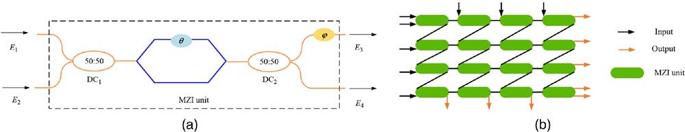
    Fig. 1. (a) Schematic diagram of programmable MZI. (b) Silicon photonic neural network based on MZI array with eight input ports and eight output ports.
    Single-layer optical interference and nonlinear element on artificial neural network.
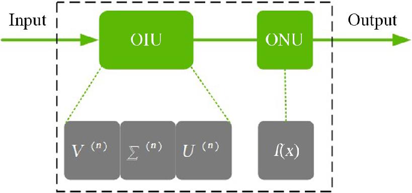
    Fig. 2. Single-layer optical interference and nonlinear element on artificial neural network.
    Patching transform of the CONV to GEMM.
    Fig. 3. Patching transform of the CONV to GEMM.
    CDC maps the CONV into the MZI unit.
    Fig. 4. CDC maps the CONV into the MZI unit.
    High-level architecture of a general-purpose scalable photonic MZI-based NPU system.
    Fig. 5. High-level architecture of a general-purpose scalable photonic MZI-based NPU system.
    CDC input for saving bandwidth.
    Fig. 6. CDC input for saving bandwidth.
    (a) CDC-output photonic chip architecture and (b) CDC-input photonic chip architecture.
    Fig. 7. (a) CDC-output photonic chip architecture and (b) CDC-input photonic chip architecture.
    End-to-end full flow simulator architecture.
    Fig. 8. End-to-end full flow simulator architecture.
    (a) Utilization of different MZI array sizes. (b) Normalized bandwidth and normalized perf/power of the NPU for different MZI sizes. (c) The accuracies of different DAC control bits.
    Fig. 9. (a) Utilization of different MZI array sizes. (b) Normalized bandwidth and normalized perf/power of the NPU for different MZI sizes. (c) The accuracies of different DAC control bits.
    The photonic chip.
    Fig. 10. The photonic chip.
    (a) Setup server. (b) Server application test.
    Fig. 11. (a) Setup server. (b) Server application test.
    ParameterRecommend
    MZI size32 × 32
    Input DAC precision4 bits
    Output ADC precision4 bits
    CDC I/O patterninput
    Total MZI number8
    MZI broadcast number4
    MZI array parallel number2
    Table 1. Summary of data set and DNN architecture.
    Li Pei, Zeya Xi, Bing Bai, Jianshuai Wang, Jingjing Zheng, Jing Li, Tigang Ning. Joint device architecture algorithm codesign of the photonic neural processing unit[J]. Advanced Photonics Nexus, 2023, 2(3): 036014
    Download Citation