
Li Pei, Zeya Xi, Bing Bai, Jianshuai Wang, Jingjing Zheng, Jing Li, Tigang Ning, "Joint device architecture algorithm codesign of the photonic neural processing unit," Adv. Photon. Nexus 2, 036014 (2023)
- Advanced Photonics Nexus
- Vol. 2, Issue 3, 036014 (2023)
Abstract
1 Introduction
In recent years, deep neural networks (DNNs) have involved large amounts of links and large data capacity, enabling the high quality of data processing. DNNs have been applied in image analysis, video tracking, language translation,1,2 etc. They are mostly deployed in electronic hardware, including the central processing unit, graphical processing unit, and tensor processor unit. However, according to the Moore’s law, the electronic devices are insufficient to cope with the explosive information crisis, due to limited complementary metal-oxide semiconductor (CMOS) fabrication techniques.3 The linearity and nonlinearity of integrated optical devices for analog signal processing can greatly improve the performance and power efficiency of these artificial intelligence (AI) workloads.4 The calculation core of the photonic neural processing unit (PNPU) is to complete matrix multiplication in a short time. That breaks the bottlenecks caused by system electronics parts. Matrix computation belongs to basic information processing. The PNPU aims to accelerate the calculation in the optical field to meet the growing demand for computing resources and capacity.5
A PNPU with consisting of a Mach–Zehnder interferometer (MZI) unit has demonstrated great progress in accelerating the DNN applications, with over 100 GHz photodetection rates and near-zero energy dissipation.3 Due to the addition of photonic elements, the PNPU has higher data processing speed than an electronic processing unit, and the amount of data that can be processed is greatly improved.6,7 The photonic characteristics allow PNPU with greater bandwidth and lower power consumption.8 The PNPU provide some performance advantages for neural network computing, such as shape factor, manufacturability, cost, mechanical stability, and high-speed modulation.9
However, the PNPU suffers a challenge in robustness due to the nonideal effects of the MZI unit, which is similar to other neuromorphic systems.4,6 The nonideal effects include the phase shift produced by the MZI unit’s low voltage control resolutions7,10 and device-level noise on the MZIs caused by the manufacturing imperfection and environment.11 Meanwhile, the small data set-based fully connected neural networks cannot reveal the accuracy loss due to the nonideal effects. The general neural processing unit (NPU) is much more complex than the fixed application NPU accelerator, and it should be configured to apply for different networks and applications. It is highly demanded to develop a methodology to evaluate PNPU with non-ideal effects. The second section of the article mainly introduces the theoretical model, including the calculation theory of MZI and DNN. The third section shows the current chip architecture, including the overall architecture and optical chip architecture. Then based on the chip, the framework of optoelectronic hybrid computing was constructed, including the simulator. Finally, the application testing was demonstrated.
2 Theoretical model
Using programmable MZI array, simple neural network functions can be realized.
2.1 MZI Unit
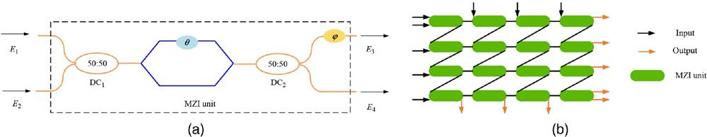
Commonly, MZI is used in optical circuits, and it usually completes the electrical or thermal modulation of photonic signals. The schematic diagram of a programmable MZI is shown in Fig. 1(a), including two 50:50 evanescent directional couplers and two phase shifters (
![]()
Figure 1.(a) Schematic diagram of programmable MZI. (b) Silicon photonic neural network based on MZI array with eight input ports and eight output ports.
Any unitary transformation can be decomposed into a group of
When the multilayer operation is to be carried out, as shown in Fig. 1(b), it realizes matrix multiplication completely optically. In each layer, the input optical signal first undergoes a linear matrix multiplication of a linear unit. The transmitted data are transmitted to the computer layer, and then feed forward and backpropagation algorithms can be trained. The weighted matrix is replaced by
![]()
Figure 2.Single-layer optical interference and nonlinear element on artificial neural network.
![]()
Figure 3.Patching transform of the CONV to GEMM.
As this section has discussed, the optical MZI unit in Fig. 1(b) performs a matrix–vector product. The different sets of vectors can perform a general matrix-matrix product (GEMM) sequentially, which is a key function in the basic linear algebra subprograms (BLAS).14
2.2 DNN with MZI Unit
Most of DNN algorithms consist of convolutional (CONV) layers and full connected layers, and they are back-to-back connected and run sequentially. The computer-intensive operations of the CONV layers and fully connected layers are CONV and vector–matrix multiplication.
There are two ways to implement the CONV operation with the MZI unit:
The CONV operation can be transformed to the GEMM operation by performing a “patching” technique, and the GEMM can be naturally operated in the optical MZI unit. The expression of the CONV layer is
Here, the input is
As shown in Fig. 3, the ‘patching’ technique works transform the CONV operation to the GEMM operation. After the kernel strides over the input image with the fixed step, we can get a bunch of the overlapped matrices, called “patches.” The patches are then rearranged to express a matrix
The other method for transforming the CONV to the GEMM is adding a CDC and an adder in the output of the MZI units. An example of 2D
A CDC and an adder are employed to complete the above transformation in Fig. 4. Every cycle’s output of adder corresponds to Eq. (3). The CDC can be configured to have different latency to support different stride sizes of the CONV. Different “add” channels of the feature map can be operated in the different MZI units in parallel. The second method is used in this study. The details will be shown in the next section.
![]()
Figure 4.CDC maps the CONV into the MZI unit.
2.3 Challenge
Due to the underlying nonideal characteristics of photonic MZI devices and arrays,15
3 Joint Device-architecture-algorithm Codesign
3.1 Architecture Design
To develop a simulator for the PNPU, a baseline architecture is required. As shown in Fig. 5, the proposed high-level architecture of a general-purpose scalable photonic MZI-based NPU system includes four parts: a photonic MZI chip, field programmable gate arrays (FPGAs) (a digital application-specific integrated circuit chip), peripheral drivers, and transimpedance amplifier (TIA) modules. The FPGA fetches input data from the host module and performs some nonlinearity operation (such as activation function and pooling) and kernel/feature data management in the double data rate and local buffer. The drivers and TIA modules can receive input images from off-chip and send the results to off-chip. The operations are carried out on a photonic chip in the form of light.
![]()
Figure 5.High-level architecture of a general-purpose scalable photonic MZI-based NPU system.
The input/output bandwidth of the photonic chip plays a significant role in the performance of the PNPU. We propose two different methods to optimize the input/output bandwidth of the photonic chip. In Sec. 2, we have introduced the hardware CDC, which will save the photonic chip’s output bandwidth by reducing the output ports number.
A broadcast and CDC method are introduced to save the input bandwidth of the photonic chip, as shown in Fig. 6. When the kernel filter shifter in the input feature map with a stride of 1, the adjacent two patches have six pixels overlap, and only three pixels are newly input. The delay chain can keep the last two cycles’ history values and output nine pixels every cycle. The input CDC can save the bandwidth about 66.7% in this case.
![]()
Figure 6.CDC input for saving bandwidth.
3.1.1 Photonic chip
The photonic chip receives the feature map data and kernel data sent from the digital chip, performs the CONV/GEMM operation, and sends the data back to the digital chip with the following steps. The photonic chip consists of the laser source, programmable logic controller, spot size convector, modulator, beam splitter, MZI arrays, delay chain, adder, and photodetector.
There are two different architectures of the photonic chip: the CDC-output photonic chip and the CDC-input photonic chip. Figure 7(a) demonstrates the CDC-output photonic chip, and it can save the chip’s output bandwidth, whereas Fig. 7(b) shows the CDC-input photonic chip, which is used to save the input bandwidth of the chip. Both transmit data by broadcasting, but the former operates at the output end and the latter works at the input end.
![]()
Figure 7.(a) CDC-output photonic chip architecture and (b) CDC-input photonic chip architecture.
3.1.2 Full-flow simulator based on design architecture
An end-to-end full-flow simulator is developed to explore the design space of the PNPU. The full-flow simulator has the following submodules (Fig. 8): a training framework tool, a photon-based NPU compiler, and a back-end evaluation tool. The full-flow simulator can support the evolution of the training and interface accuracy and support the evaluation of the power, performance, and area (PPA) of the PNPU.
![]()
Figure 8.End-to-end full flow simulator architecture.
The training framework is different from the traditional digital NPU training framework; there are three major differences. At first, the control weight of the MZI array should be calculated from a complex SVD operation after getting the traditional weight matrix. Next, our interface system is a hybrid photonic–electronic system that can implement different amounts of precision of the interface. The training framework should consider the mix precision. Then the nonideal effects of the MZI array must be taken into consideration, which can augment the robustness of the interface results. We adapt a noise-aware training and quantization scheme19 to enhance the robustness of the PNPU.
The compiler’s target is to optimize the computation and unleash the computation power of PNPU by mapping the model into a highly optimized commands/instructions sequence. It consists of three parts of submodules. They are the optimizer, the parser, and the partitioner. The optimizer prunes the network structure and fine-tunes the weight value so it can reduce the model complexity and improve the inference efficiency. The parser takes the pruned network structure and the hardware configuration as input. It can transform the network structure into computation graph intermediate representation, control flow, and data flow information. The partitioner chooses the best parallelism model and maps the different layers of operation into electronic or photonic logic to perform parallelism. The compiler should also know the hardware configuration to make the best decision. The output data are the control flow information and internally defined commands, and they will be sent to the back-end simulator.
The back-end simulator is used to evaluate two aspects of the design. The first one is the PPA of the PNPU. The second one is the inference accuracy. The PPA evaluation tool models the full design of the PNPU system, which includes buffers, DAC, ADC, modulator, TIA, digital logic, and a laser. The accuracy evaluation tool is used to simulate the forward inference accuracy. It does not directly model the nonidealities of devices. Instead, it extracts the MZI array operation model and adds some random shifter/noise to the output of the MZI operation result.
3.2 Optimization of Algorithm
The photonic chip’s architecture and MZI array size have a big influence on the performance of the PNPU system. The multiply accumulate (MAC) utilization is determined by the MZI array size and the network structure, and the required input/output bandwidth depends on the photonic architecture and MZI array size. Therefore, we use the full-flow simulator to get the optimized MZI array size for the PNPU. The input data set for the first network (Net-1) is “MNIST.” The size of the MZI array is
As the size of the MZI array increases, the utilization ratio of the MZI unit decreases, as shown in Fig. 9(a). The MZI utilization is also related to the DNN architecture, and the Net-3 decreases less than the Net-1 and Net-2. However, when the MZI array size increases, the required bandwidth increases, but the perf/power decreases when the size is larger than 24 [Fig. 9(b)]. The power of the laser and peripheral circuit increases rapidly when the size of the MZI array increases. Thus, to make a trade-off among the utilization ratio, bandwidth, and perf/power, the MZI array size should be smaller than
![]()
Figure 9.(a) Utilization of different MZI array sizes. (b) Normalized bandwidth and normalized perf/power of the NPU for different MZI sizes. (c) The accuracies of different DAC control bits.
As discussed in Sec. 2.3, the nonidealities of the MZI unit and the DAC accuracy significantly affect the computing accuracy of the NPU. We use the full-flow simulator to evaluate the effects of the nonidealities and voltage control precision. The inference accuracy results of different voltage controls from 3 to 6 bits DAC resolution are shown in Fig. 9(c). The fewer bits of voltage control DAC, the lower accuracy will be gotten. Consequently, the final network is shown in Table 1.
| Parameter | Recommend |
| MZI size | 32 × 32 |
| Input DAC precision | 4 bits |
| Output ADC precision | 4 bits |
| CDC I/O pattern | input |
| Total MZI number | 8 |
| MZI broadcast number | 4 |
| MZI array parallel number | 2 |
Table 1. Summary of data set and DNN architecture.
3.3 Construction and Application of Server
Based on the architecture design and algorithm optimization of the above photonic chip, we have completed the chip fabrication. The photonic chip cut from a wafer is shown in Fig. 10.
![]()
Figure 10.The photonic chip.
The server [Fig. 11(a)] is built based on the architecture in Fig. 5, and it is tested in a data center [Fig. 11(b)]. In the test tasks of video recognition and image segmentation, the average test accuracy exceeds 98%, and the computing power exceeds 100TOPS.
![]()
Figure 11.(a) Setup server. (b) Server application test.
4 Conclusion
In this article, we present a multidirectional collaborative design scheme from device to circuit to algorithm. We have developed an end-to-end photonic neural network simulator that can monitor from multiple directions and visually display the results of data flow. On this basis, we have completed the design and fabrication of a photonic chip and developed a set of servers that can be used for AI tasks. This provides a new idea for follow-up development and utilization of photonic chips. On-chip integrated photonic circuits are an ideal platform for AI. However, to transform the experimental demonstration into a real processor, it is necessary to overcome some key emerging technologies, such as computational bandwidth, intelligent control strategy, and all-optical neural network. In short, the PNPU has great potential in emerging AI applications, but how to comprehensively improve the optical computing system is still challenge.
Acknowledgment
Acknowledgment. This work was supported by the National Natural Science Foundation of China (Grant No. 61827817).
Biographies of the authors are not available.
References
[6] A. S. Rekhi et al. Analog/mixed-signal hardware error modeling for deep learning inference(2019).
[7] L. Song et al. PipeLayer: a pipelined ReRAM-based accelerator for deep learning, 541-552(2017).
[15] D. Dang et al. BPLight-CNN: a photonics-based backpropagation accelerator for deep learning, 17(2021).
[17] A. Krizhevsky, G. Hinton. Learning multiple layers of features from tiny images. Handbook of Systemic Autoimmune Diseases, 2(2009).
[18] J. Deng et al. ImageNet: a large-scale hierarchical image database(2009).


Set citation alerts for the article
Please enter your email address

© Copyright 2018-2021 | Chinese Laser Press. All Rights Reserved 沪ICP备15018463号-20