
Shuo Zhang, Ge Mu, Jie Cao, Yuning Luo, Qun Hao, Menglu Chen, Yimei Tan, Pengfei Zhao, Xin Tang, "Single-/fused-band dual-mode mid-infrared imaging with colloidal quantum-dot triple-junctions," Photonics Res. 10, 1987 (2022)
- Photonics Research
- Vol. 10, Issue 8, 1987 (2022)
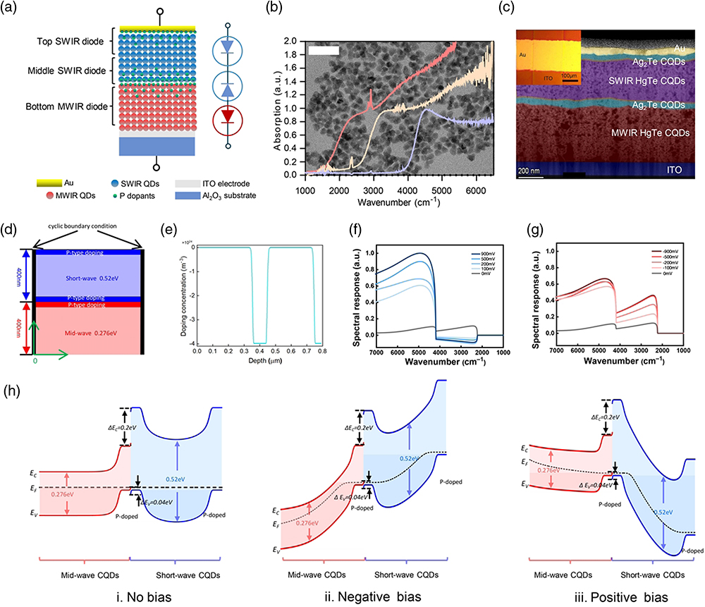
Fig. 1. Infrared spectral fusion technology. (a) Illustration of dual-mode colloidal quantum-dot photodetectors and equivalent circuits of triple-junction structure. (b) Transmission electron microscopy and absorption of HgTe colloidal quantum dots with various sizes. The scale bar is 10 nm. (c) Cross-sectional transmission electron microscopy image of the dual-mode detectors. Inset is a microscope image of the dual-mode detectors whose area is defined by the overlap between the top gold electrode and the bottom ITO electrode. (d) The simulation model of the HgTe CQDs dual-mode infrared detector. (e) Distribution of doping concentration. (f), (g) The simulation spectral responses of the dual-mode infrared detector under negative bias and positive bias. (h) Simulated energy band diagram of dual-mode triple-junction photodetectors under zero, negative, and positive bias voltage.

Fig. 2. Characterization of dual-mode detectors. Bias-dependent spectral response under (a) positive and (b) negative bias voltages. (c) Pulsed photoresponse to short-wave infrared, mid-wave infrared, and mixed illumination. (d) I-V characteristics of the dual-mode detector under blackbody irradiation at various distances. (e) Bias-dependent responsivity and detectivity of a dual-mode photodetector. (f) Linear dynamic range measurement of dual-mode detectors in the single-band mode and the fused-band mode. (g) Frequency response measurement of dual-mode detector. The inset is the measured response time of the dual-mode detector. (h) Photoresponse of the dual-mode detector biased with a positive and negative square wave at the frequency of 500 kHz. (i) Measured fused-band to single-band response ratio. The red dashed line is the measured ratio with a calibrated blackbody.
Fig. 3. Dual-mode infrared imaging. (a) Illustration of single-pixel scanning imaging setup. (b) Visible image, short-wave infrared, mid-wave infrared, and fused-mode images of two soldering irons. (c) Visible image, short-wave infrared, mid-wave infrared, and fused-mode images of two cups of water.
Fig. 4. Resonant cavity-enhanced dual-mode operation. (a) Illustration of resonant cavity structure. The inset on the right side is the simulated light E -field mapping in the cavity. (b) Simulated light absorption mapping in dual-mode detectors with and without a cavity. (c) Simulated spectral absorption at various spacer thicknesses. (d) Measured spectral enhancement ratio at various spacer thicknesses. (e) Photocurrents from dual-mode detectors with and without a cavity.


Set citation alerts for the article
Please enter your email address

© Copyright 2018-2021 | Chinese Laser Press. All Rights Reserved 沪ICP备15018463号-20