
Shuo Zhang, Ge Mu, Jie Cao, Yuning Luo, Qun Hao, Menglu Chen, Yimei Tan, Pengfei Zhao, Xin Tang, "Single-/fused-band dual-mode mid-infrared imaging with colloidal quantum-dot triple-junctions," Photonics Res. 10, 1987 (2022)
- Photonics Research
- Vol. 10, Issue 8, 1987 (2022)
Abstract
1. INTRODUCTION
Extensive efforts have been made in the infrared ranges with the desire to achieve multiband or hyperspectral imaging. Going beyond human vision capability, infrared can provide objects’ important information such as molecular composition and thermal distribution. For better target recognition and identification, there are strong demands for combining images from different spectral bands, which is also known as spectral image fusion technology [1]. This image from fused spectral bands can provide a more accurate understanding of the surrounding information compared to single spectral data. Despite continuous efforts on sophisticated fusion algorithms [2–4], registration error inevitably presents due to the mismatch of pixel size, array size, and optical imaging axis between separate imagers.
The simple solution to this problem would be an imager that responds to distinct spectral ranges and fuse signals on the pixel level. However, the spectral sensing ranges of imagers are mainly defined by their materials (e.g., Si for 0.4–0.7 nm at visible, InGaAs for 1.5–1.7 μm at short-wave infrared, and HgCdTe for 3–12 μm at mid-infrared) and combination of different materials into the same pixel vertically or horizontally is hindered by the lattice mismatch and incompatibility between fabrication processes.
As an alternative to epitaxial semiconductors, colloidal quantum dots (CQDs), over the past years, have been extensively explored for their unique properties such as size-tunable optical features and the ease of fabrication as solution-processable materials [5]. With continuous advancements in synthesis, the sensing ranges of CQDs have been gradually extended to access mid-infrared [6,7] with state-of-the-art device performance rivaling to their counterparts of bulk semiconductors. Among colloidal nanomaterials, mercury chalcogenides (HgX, X represents S, Se, Te) CQDs have demonstrated, so far, the highest spectral tunability. Short-wave infrared (SWIR) photovoltaic detectors with detectivity
Sign up for Photonics Research TOC. Get the latest issue of Photonics Research delivered right to you!Sign up now
To address such technological challenges and meet the growing demands for fused multispectral infrared imaging, we propose the development of a dual-mode colloidal quantum-dot infrared detector, which provides unprecedented bias-dependent single-band SWIR imaging mode and fused-band SWIR/MWIR mode. The SWIR mode provides details of the scene such as visible light, while the fused SWIR/MWIR mode adds thermal information directly to the SWIR image on the detector level. Our results show that a triple-junction structure arranged in alternating polarity is the key to fused response. The dual-mode detectors show
2. MATERIALS AND METHODS
A. Device Physics and Operation Principle
The study of infrared CQDs starts from photoconductive and single-junction photovoltaic device configuration, which clearly exhibits no spectral selectivity or fusion ability. Inspired by the band engineering of epitaxial semiconductors [16] (HgCdTe, quantum wells, Type II superlattice), a two-color CQDs detector with vertically stacked “back-to-back” diode configuration was introduced and demonstrated bias-tunable spectral response [17]. However, they still output single-band data at a fixed bias and require post-processing for image fusion. It is true that a three-terminal detector with a third middle common contact could possibly output images from two spectral bands simultaneously, but that inevitably increases structural complexity and cost of readout circuits.
The difficulty in fused response lies in the need that photocurrents from different spectral bands need to be combined either in series or in parallel with high efficiency. Our initial attempts include (1) the combination of a photoconductive SWIR layer with photovoltaic MWIR junction, (2) photovoltaic junction with mixed SWIR/MWIR CQDs solution, (3) parallelly stacked MWIR and SWIR junction, and (4) tandem SWIR/MWIR configuration. Despite that fused-band spectral response was indeed measured, they all showed low detectivity below
To realize efficient fused-band response, we designed a new device architecture by stacking three rectifying colloidal quantum-dot homojunctions, as shown in Fig. 1(a). The top SWIR photodiode and bottom MWIR photodiode have the same polarity. An SWIR photodiode with opposite polarity is sandwiched in the middle, which plays a central role in the fused-band operation and provides an additional single-band response mode. When the triple-junction detector works in the fused-band mode, the middle SWIR diode is turned off and provides an essential interfacial charge transport channel for photogenerated carriers. By changing the bias direction, both the top SWIR photodiode and bottom MWIR photodiode are closed. The triple-junction detector then outputs single-band SWIR signals. With two terminals, such detectors allow unprecedented bias-polarity-dependent dual-mode operation. The construction of the dual-mode detectors starts from the colloidal synthesis of HgTe CQDs that access the SWIR (
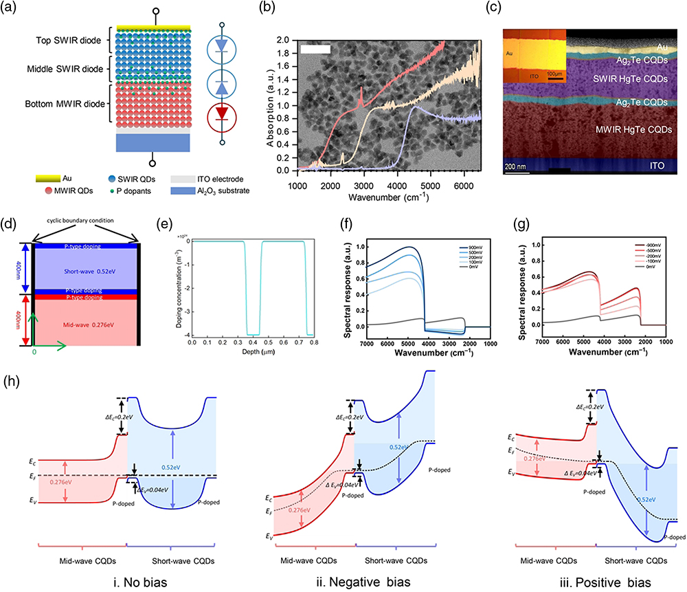
Figure 1.Infrared spectral fusion technology. (a) Illustration of dual-mode colloidal quantum-dot photodetectors and equivalent circuits of triple-junction structure. (b) Transmission electron microscopy and absorption of HgTe colloidal quantum dots with various sizes. The scale bar is 10 nm. (c) Cross-sectional transmission electron microscopy image of the dual-mode detectors. Inset is a microscope image of the dual-mode detectors whose area is defined by the overlap between the top gold electrode and the bottom ITO electrode. (d) The simulation model of the HgTe CQDs dual-mode infrared detector. (e) Distribution of doping concentration. (f), (g) The simulation spectral responses of the dual-mode infrared detector under negative bias and positive bias. (h) Simulated energy band diagram of dual-mode triple-junction photodetectors under zero, negative, and positive bias voltage.
B. Device Fabrication
The synthesis of HgTe CQDs and
C. Photoresponse Characterization
The detector was placed in a cryostat for performance characterization. Responsivity was measured using a calibrated blackbody source at 600°C. The photon flux on the detector was determined by the area of the detector, the area of the blackbody, the distance between the detector and the blackbody, and the spectrum of the blackbody radiation. The photocurrent was amplified first by a preamplifier (Femto DLA-200) and the noise was measured with a spectrum analyzer.
D. Experimental Processes of Scanning Imaging
The single-pixel scanning system consists of imaging objects, an infrared lens, motorized XY linear stages, a dual-mode photodetector, an amplifier, a data acquisition card, and software. The lens is mounted on the motorized XY stage, the imaging object is located in
3. RESULTS AND DISCUSSION
A. Device Simulation
To investigate the device physics and operation mechanism, the structure, energy band, and performance of the dual-mode detectors were simulated with the finite element analysis method using the semiconductor module and wave optics module. Figure 1(d) shows the schematic diagram of the simulation model, in which the lower left corner is the origin of coordinates, and the two sides are periodic boundary conditions. The mid-wave HgTe CQDs and short-wave HgTe CQDs both with a thickness of 400 nm were stacked vertically with bandgaps of 0.52 eV and 0.27 eV.
B. Characterization of Dual-Mode Operation
The dual-mode detectors were mounted in a cryostat and cooled down to
![]()
Figure 2.Characterization of dual-mode detectors. Bias-dependent spectral response under (a) positive and (b) negative bias voltages. (c) Pulsed photoresponse to short-wave infrared, mid-wave infrared, and mixed illumination. (d)
The simulated energy band diagram suggested efficient photocarriers transportation from one diode without the need for current balance to the other side of detectors. This is experimentally confirmed by measuring photoresponse to chopped SWIR light, MWIR light, and SWIR and MWIR light. The sum of photocurrents from SWIR and MWIR light approximates the photocurrents under the illumination of both SWIR and MWIR, which is clear evidence that photocarriers generated inside the detector can be generated, add, and move freely [Fig. 2(c)]. To calculate the responsivity and detectivity, the I-V characteristics of the dual-mode detector were measured with a calibrated blackbody with a temperature of 600°C at various distances [Fig. 2(d)]. The photoresponse in the fused-band mode is around 3 times higher than in single-band SWIR mode, which matches the spectral radiation of the light source. We noticed that at
For infrared photodetectors, detectivity is the most important figure of merit as it is associated with the signal-to-noise ratio. The
By modulating the bias voltage, the SWIR and fused SWIR/MWIR signals can be read sequentially during a short time interval. The representative modulated photoresponses are shown in Fig. 2(h). The orange and blue shaded areas denote the magnitude of MWIR and SWIR signals, from which the single-band/fused-band response ratio can be calculated. The advantages of dual-mode detection are obvious. Unlike a single-band detector, such a dual-mode detector can precisely determine objects’ temperature based on their emission spectrum. This method is independent of the magnitude of optical power or distance between the detector and the measured objects. As shown in Fig. 2(i), based on the calibrated fused-band mode/single-band mode signal ratio with a blackbody, the temperature of human hands, hotplates, soldering irons, and heat guns can be measured, highlighting the fact that the dual-mode detector can be used for absolute and remote temperature measurement. The blackbody curve is measured and calculated by using the blackbody as the light source. The ratio of photocurrents between the single-band mode and fused-band mode was recorded as the temperature of the blackbody changed.
It is true that bias-dependent dual-band detectors have been demonstrated by using two-dimensional materials [22–24], perovskites [25], and organic junctions [26], and excellent performance with detectivity above
C. Dual-Mode Infrared Imaging
The dual-mode operation enables our detectors with functionalities of both night vision and thermal imaging-enhanced night vision capability. To give a visual demonstration, the dual-mode detectors were integrated with a single-pixel scanning system for infrared imaging [Fig. 3(a)]. As the projected images scanned over the detectors, the photocurrents were amplified and recorded by a high-speed acquisition card at a sampling rate of 5 kHz.
![]()
Figure 3.Dual-mode infrared imaging. (a) Illustration of single-pixel scanning imaging setup. (b) Visible image, short-wave infrared, mid-wave infrared, and fused-mode images of two soldering irons. (c) Visible image, short-wave infrared, mid-wave infrared, and fused-mode images of two cups of water.
As shown in Fig. 3(b), two soldering irons with the temperatures of 200°C and 25°C were imaged. When positively biased, the detector works in the single-band SWIR mode and the two soldering irons, including the one blocked behind a silicon wafer, were clearly captured with a tungsten lamp as the light source. By flipping the polarity of bias voltage, the detector works in the SWIR/MWIR fused mode. Without external light, the fused-mode detector can sense the thermal emission from objects and give the thermal distribution of the scene, in which only the “hot spot” on the soldering iron is noticeable. These results further confirmed the advantageous feature that no photocurrent balance is needed for the triple-junction structure between two different sensing bands. After adding the external tungsten light, the fused-band detectors can spontaneously add the signal from two different bands and output fused photocurrent. As shown in the fourth row of Fig. 3(b), both MWIR thermal information and SWIR reflected image were captured.
As shown in Fig. 3(c), two cups of water with different temperatures were also imaged and showed consistent phenomena. It is worth noting that obscure silicon wafers can be seen through, and transparent water is black in SWIR images, highlighting the potential for SWIR in the application of semiconductor inspection and chemical analysis.
The noise equivalent temperature difference (NETD) is measured with two cups above. The NETD is defined as
D. Spectral and Spatial Light Manipulation for Enhanced Performance
Optical manipulation with plasmonic metallic structures [27,28], photonic crystals [29,30], meta-surfaces, and immersion lenses has been widely used in photodetectors to boost device performance by increasing light absorption. Usually, responsivity and quantum efficiency can be improved by near-field enhancement or light concentration. However, such structures are not suitable for a multispectral infrared detector or our dual-mode detectors. The first problem is that such configurations often give narrow spectral enhancement wavelength and cannot achieve improvements over the multiwavelength or broadband spectrum. More importantly, if the optical enhancement relies on near-field effects within sub-wavelength regions, it is not suitable for multiband or multimode photodetectors with layered functional structures where the localized light manipulation cannot spatially reach the layered sensing areas.
To further improve our device performance, we integrated the dual-mode detector into a well-designed resonance cavity which can spectrally and spatially match the light distribution inside the detectors with the triple sensing junctions. The detectivity and spectral selectivity can be improved at the same time. The resonant cavity is in Fabry–Perot configuration by simply adding an optical spacer and highly reflective gold mirror under the dual-mode detectors, as shown in Fig. 4(a). In a typical dual-mode detector, the thicknesses of SWIR and MWIR CQDs layers are both around 400 nm. The absorption edges were set to be 2.25 and 4 μm, respectively. As shown in the simulated light absorption distribution mapping in Fig. 4(b), with correct spacer thickness, the light absorption can be tuned to spatially match the depletion region of the junctions. For light with a wavelength of 2.25 μm, the maximum absorption region is near the top and bottom areas of SWIR CQDs, where strong built-in potentials are induced to separate photocarriers. For light with a wavelength of 4 μm, the overall absorption across the whole sensing region was also notably enhanced. Therefore, the spatial and spectral modulation of light distribution inside the dual-mode detectors leads to enhanced light absorption and the spectral absorption enhancement can be tuned by optical spacer thickness. This is confirmed by both simulation and experimental results [Figs. 4(c) and 4(d)]. Figure 4(c) shows the simulated spectral absorption of detectors with various spacer thicknesses. The simulation results revealed obvious spacer thickness-dependent absorption peaks. The spectral enhancement ratio between detectors with and without resonant cavities was also experimentally measured and demonstrated
![]()
Figure 4.Resonant cavity-enhanced dual-mode operation. (a) Illustration of resonant cavity structure. The inset on the right side is the simulated light
4. CONCLUSIONS
Photodetection of light generated from different mechanisms (blackbody radiations, specularly reflected and transmitted light from objects) represents enormous and distinct optical information including thermal distribution, molecular composition, and surface texture. By fusing information on the detector level, fused images without registration error can be achieved, which is a great advantage over current image fusion methods with separate imagers. In this work, we constructed a dual-mode photodetector with three alternatingly stacked photodiodes, which exhibits remarkable dual-mode operation. By changing the polarity of bias voltage, the triple-junction detectors can be tuned between single-band detectors and fused-band detectors. The single-band mode detects short-wave infrared while the fused mode can detect and fuse photons from both short-wave and mid-wave infrared. Optical information from different spectral bands can be added together without post-processing or image algorithms. The addition of the middle diode with opposite polarity is the key to this unprecedented dual-mode operation by providing an interfacial carrier transport channel for fused-band response and single-band SWIR detection. The detectivity for the single-band SWIR mode and the fused-band SWIR/MWIR mode can be as high as
References
[1] J. Ma, W. Yu, P. Liang, C. Li, J. Jiang. FusionGAN: a generative adversarial network for infrared and visible image fusion. Inf. Fusion, 48, 11-26(2019).
[2] J. Ma, J. Zhao, Y. Ma, J. Tian. Non-rigid visible and infrared face registration via regularized Gaussian fields criterion. Pattern Recogn., 48, 772-784(2015).
[3] S. G. Kong, J. Heo, F. Boughorbel, Y. Zheng, B. R. Abidi, A. Koschan, M. Yi, M. A. Abidi. Multiscale fusion of visible and thermal IR images for illumination-invariant face recognition. Int. J. Comput. Vis., 71, 215-233(2007).
[4] J. Ma, C. Chen, C. Li, J. Huang. Infrared and visible image fusion via gradient transfer and total variation minimization. Inf. Fusion, 31, 100-109(2016).
[5] M. V. Kovalenko. Opportunities and challenges for quantum dot photovoltaics. Nat. Nanotechnol., 10, 994-997(2015).
[6] S. Keuleyan, E. Lhuillier, P. Guyot-Sionnest. Synthesis of colloidal HgTe quantum dots for narrow mid-IR emission and detection. J. Am. Chem. Soc., 133, 16422-16424(2011).
[7] S. Keuleyan, E. Lhuillier, V. Brajuskovic, P. Guyot-Sionnest. Mid-infrared HgTe colloidal quantum dot photodetectors. Nat. Photonics, 5, 489-493(2011).
[8] X. Tang, M. M. Ackerman, G. Shen, P. Guyot-Sionnest. Towards infrared electronic eyes: flexible colloidal quantum dot photovoltaic detectors enhanced by resonant cavity. Small, 15, 1804920(2019).
[9] M. M. Ackerman, X. Tang, P. Guyot-sionnest. Fast and sensitive colloidal quantum dot mid-wave infrared photodetectors. ACS Nano, 12, 7264-7271(2018).
[10] X. Tang, M. M. Ackerman, P. Guyot-Sionnest. Thermal imaging with plasmon resonance enhanced HgTe colloidal quantum dot photovoltaic devices. ACS Nano, 12, 7362-7370(2018).
[11] X. Wang, G. I. Koleilat, J. Tang, H. Liu, I. J. Kramer, R. Debnath, L. Brzozowski, D. A. R. Barkhouse, L. Levina, S. Hoogland, E. H. Sargent. Tandem colloidal quantum dot solar cells employing a graded recombination layer. Nat. Photonics, 5, 480-484(2011).
[12] J. Tang, X. Wang, L. Brzozowski, D. A. R. Barkhouse, R. Debnath, L. Levina, E. H. Sargent. Schottky quantum dot solar cells stable in air under solar illumination. Adv. Mater., 22, 1398-1402(2010).
[13] A. K. Rath, M. Bernechea, L. Martinez, G. Konstantatos. Solution-processed heterojunction solar cells based on p-type PbS quantum dots and n-type Bi2S3 nanocrystals. Adv. Mater., 23, 3712-3717(2011).
[14] J. Qu, M. Weis, E. Izquierdo, S. G. Mizrahi, A. Chu, C. Dabard, C. Gréboval, E. Bossavit, Y. Prado, E. Péronne, S. Ithurria, G. Patriarche, M. G. Silly, G. Vincent, D. Boschetto, E. Lhuillier. Electroluminescence from nanocrystals above 2 μm. Nat. Photonics, 16, 38-44(2022).
[15] A. Rogalski. History of infrared detectors. Opto-Electron. Rev., 20, 279-308(2012).
[16] A. Rogalski, J. Antoszewski, L. Faraone. Third-generation infrared photodetector arrays. J. Appl. Phys., 105, 091101(2009).
[17] X. Tang, M. M. Ackerman, M. Chen, P. Guyot-Sionnest. Dual-band infrared imaging using stacked colloidal quantum dot photodiodes. Nat. Photonics, 13, 277-282(2019).
[18] S. Zhang, M. Chen, G. Mu, J. Li, Q. Hao, X. Tang. Spray-stencil lithography enabled large-scale fabrication of multispectral colloidal quantum-dot infrared detectors. Adv. Mater. Technol., 7, 2101132(2021).
[19] E. H. Sargent. Infrared photovoltaics made by solution processing. Nat. Photonics, 3, 325-331(2009).
[20] S. Sista, M. H. Park, Z. Hong, Y. Wu, J. Hou, W. L. Kwan, G. Li, Y. Yang. Highly efficient tandem polymer photovoltaic cells. Adv. Mater., 22, 380-383(2010).
[21] J. Y. Kim, K. Lee, N. E. Coates, D. Moses, T. Q. Nguyen, M. Dante, A. J. Heeger. Efficient tandem polymer solar cells fabricated by all-solution processing. Science, 317, 222-225(2007).
[22] A. Hwang, M. Park, Y. Park, Y. Shim, S. Youn, C. Lee, H. B. Jeong, H. Y. Jeong, J. Chang, K. Lee, G. Yoo, J. Heo. Visible and infrared dual-band imaging via Ge/MoS2 van der Waals heterostructure. Sci. Adv., 7, eabj2521(2021).
[23] M. Dai, H. Chen, R. Feng, W. Feng, Y. Hu, H. Yang, G. Liu, X. Chen, J. Zhang, C. Xu, P. Hu. A dual-band multilayer InSe self-powered photodetector with high performance induced by surface plasmon resonance and asymmetric Schottky junction. ACS Nano, 12, 8739-8747(2018).
[24] J. Deng, L. Zong, W. Bao, M. Zhu, F. Liao, Z. Guo, Y. Xie, B. Lu, J. Wan, J. Zhu, R. Peng, Y. Chen. Integration of MoS2 with InAlAs/InGaAs heterojunction for dual color detection in both visible and near-infrared bands. Adv. Opt. Mater., 7, 1901039(2019).
[25] H. Kim, W. Kim, Y. Pak, T. J. Yoo, H. W. Lee, B. H. Lee, S. Kwon, G. Y. Jung. Bias-modulated multicolor discrimination enabled by an organic–inorganic hybrid perovskite photodetector with a p-i-n-i-p configuration. Laser Photon. Rev., 14, 2000305(2020).
[26] Z. Lan, Y. Lei, W. Kin, E. Chan, S. Chen, D. Luo, F. Zhu. Near-infrared and visible light dual-mode organic photodetectors. Sci. Adv., 6, eaaw8065(2020).
[27] B. Zhu, M. Chen, S. V. Kershaw, A. L. Rogach, N. Zhao, H. K. Tsang. Integrated near-infrared photodetector based on colloidal HgTe quantum dot loaded plasmonic waveguide. Conference on Lasers and Electro-Optics Pacific Rim (CLEO-PR), 1-3(2017).
[28] X. Tang, G. F. Wu, K. W. C. Lai. Plasmon resonance enhanced colloidal HgSe quantum dot filterless narrowband photodetectors for mid-wave infrared. J. Mater. Chem. C, 5, 362-369(2017).
[29] A. C. Arsenault, T. J. Clark, G. Von Freymann, L. Cademartiri, R. Sapienza, J. Bertolotti, E. Vekris, S. Wong, V. Kitaev, I. Manners, R. Z. Wang, S. John, D. Wiersma, G. A. Ozin. From colour fingerprinting to the control of photoluminescence in elastic photonic crystals. Nat. Mater., 5, 179-184(2006).
[30] V. Reboud, N. Kehagias, M. Zelsmann, M. Striccoli, M. Tamborra, M. L. Curri, A. Agostiano, D. Mecerreyes, J. A. Alduncín, C. M. S. Torres. Nanoimprinted photonic crystals for the modification of the (CdSe)ZnS nanocrystals light emission. Microelectron. Eng., 84, 1574-1577(2007).


Set citation alerts for the article
Please enter your email address

© Copyright 2018-2021 | Chinese Laser Press. All Rights Reserved 沪ICP备15018463号-20