Abstract
Probing the optical properties of molybdenum disulfide (MoS2) is vital to its application in plasmon-enhanced spectroscopy, catalysts, sensing, and optoelectronic devices. In this paper, we theoretically studied the Raman and fluorescence properties of monolayer MoS2 using tip-enhanced spectroscopy (TES). In the strong-coupling TES system, the Raman and fluorescence enhancement factors can be turned to as high as 4.5×10⁸ and 3.3×10³, respectively, by optimizing the tip–MoS2-film distance. Our theoretical results not only help to deeply understand the TES properties of monolayer MoS2, but also provide better guidance on the applications of the novel two-dimensional material.1. INTRODUCTION
Unique optical and electronic properties make molybdenum disulfide () more attractive for its applications in sensing, catalysts, and optoelectronic devices [1–6]. As a novel semiconductor material, bulk presents an indirect bandgap of 1.3 eV, while monolayer exhibits a direct bandgap of 1.8 eV, which is demonstrated in theory [7]. Decreasing the thickness of not only changes the bandgap, but also improves the photoluminescence (PL) intensity, which was detected experimentally [8]. Because of the distinctive optical properties of strong absorption and PL intensity, monolayer shows better application prospects than does bulk . With the development of -based studies, more characterization techniques are required to further study the optical properties of monolayer .
Surface plasmon resonance (SPR) of a metal nanostructure largely enhances the light–exciton interaction in the near field, resulting in plasmon-enhanced phenomena such as Raman, fluorescence, and nonlinear effects [9–12]. Recent studies reveal that Ag core- shell nanoparticles can greatly improve the fluorescence of exfoliated sheets [13]. In core–shell nanostructures, the interaction distance between the emitter and metal has great impact on both PL intensity and fluorescence image. However, the ultrashort interaction distance is difficult to precisely control for actual core–shell substrates, leading to uncontrollable and unstable spectroscopy signals. Furthermore, optical image quality should be further improved by breaking the optical diffraction limit of the instrument. In this regard, the tip-enhanced spectroscopy (TES) configuration is the ideal substrate for the study of monolayer , in which scanning probe microscopy (SPM) is used to preciously control the metal tips [14,15]. More importantly, nano-spatial resolution can be offered by the TES technique, where the electromagnetic field energy is highly confined into the nanogap between the tip and the substrate [16,17].
Previous studies show both bulk and monolayer can serve as the Raman substrates, where the former exhibits electromagnetic enhancement, while the latter utilizes chemical enhancement [18–20]. In addition, some efforts have been devoted to the optical properties of monolayer , such as PL, electroluminescence (EL), Raman scattering, and high-resolution optical images. Relevant studies demonstrate that the quantum effect and the coverage of metal nanoparticles intensely influence the nanoimage and molecular signal of [21,22]. The crystal graphic orientation and structure defects of monolayer can be identified by Raman spectroscopy and near-field PL images, respectively [23,24]. EL of monolayer shows that the same excited state at 1.8 eV emerges in absorption, PL, and EL spectroscopies [25]. For TES of , there are still many unsolved scientific issues, such as the enhancement mechanism of -TES. Most studies of were performed using the specific wavelength without considering wavelength scanning. However, wavelength-scanned TES results are of great importance to fully understand the spectroscopy properties of , and provide better guidance for experiments. Furthermore, radiative and nonradiative decay processes should be systematically studied to better understand the fluorescence properties of monolayer .
In this paper, we devote ourselves to studying the wavelength-scanned TES of monolayer in theory for the first time, to the best of our knowledge. Dependence of Raman and fluorescence enhancements on the tip–-film distance was investigated by the three-dimensional finite-difference time-domain (3D-FDTD) method. The gap-mode TES provides huge enhancement factors (EFs) of Raman and fluorescence up to and , respectively, at the optimal tip–-film distance of 1.0 nm. The fluorescence enhancement mechanism of monolayer was studied in detail by analyzing the radiative and nonradiative decay rates, as well as the quantum yield in the presence of metal. Two cases involving Stokes shift and non-Stokes shift were respectively considered to discuss the fluorescence enhancement of monolayer . We believe the calculation results will be a good reference for not only better understanding the TES enhancement mechanism of monolayer , but also guiding the rational construction of -based optoelectronic devices with high efficiency.
2. CALCULATION MODEL AND METHOD
Here, a TES configuration was chosen to study the Raman and fluorescence enhancement of monolayer . Figure 1 shows the calculated TES system, which consists of an Ag tip over the Ag substrate that is covered with monolayer . The side illumination mode is used where the electric field amplitude and incident angle of the -polarized plane wave are 1.0 V/m and 60°, respectively. The apex radius and the full cone angle of the Ag tip are set as 15 nm and 20°, respectively. The thickness of film is set as 1 nm. The tip–-film and tip–substrate distances are denoted by and , as shown in Fig. 1. The simulation region is set at in 3D, and all boundaries adopt perfectly matched layer (PML) boundary conditions to avoid disturbance of the boundary reflection. Optical constants for silver and were taken from the literature [26,27].
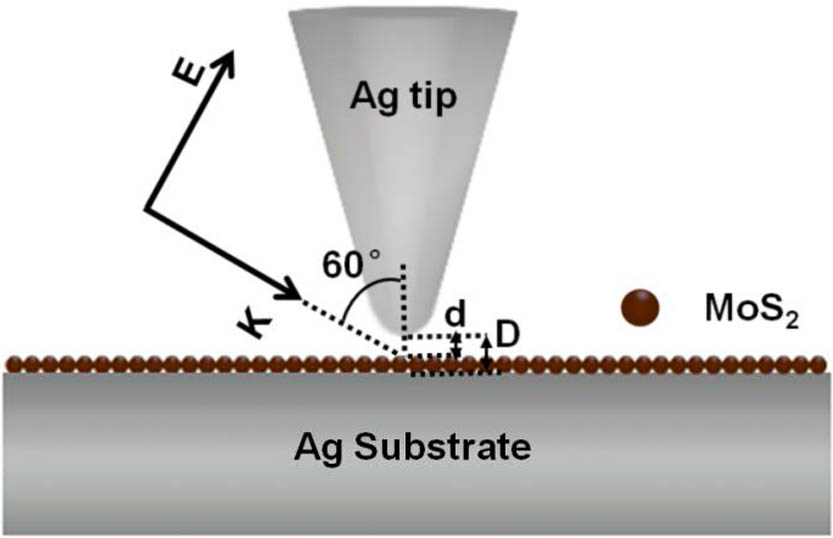
Figure 1.Schematic illustration of TES configuration using the Ag tip and a substrate with monolayer on the surface.
To quantitatively analyze the fluorescence enhancement mechanism of monolayer , the radiative and nonradiative decay processes were calculated by the 3D-FDTD method. Here, an electric dipole source was used to model the excited molecule that behaves as an oscillating electric dipole. The decay rate enhancement can be inferred from the relationship [28] where and are decay rate and radiated power in the presence of the TES configuration. The subscript 0 shows that the molecule is in free space. In our calculations, we set two monitor boxes to collect the data of total and radiated power of the electric dipole in the TES system, and thus finally calculate the radiative () and nonradiative () decay enhancement. The relationship among the total (), radiative, and nonradiative decay enhancement can be given as
Fluorescence enhancement arises mainly from the comprehensive contributions of excitation and emission processes. A localized plasmonic field can provide huge excitation enhancement (, where and are local and incident electric field, respectively) and radiative decay rate. The emission enhancement embodies the change of the quantum yield of monolayer in the presence of a TES configuration. The quantum yield () can be defined as
Therefore, we can define the fluorescence EF as where and are the excitation and emission frequencies, respectively. The details of the calculation method can be found anywhere [28–31].
3. RESULTS AND DISCUSSION
Wavelength-scanned electric field enhancement () offers clear characterization of the SPR properties of metal nanostructures from the near field. To clarify the SPR properties of TES, the Ag-tip–Ag-substrate-distance-dependent electric field enhancement of the TES configuration with () and without (, 2 nm) monolayer is presented in Fig. 2(a). The apex radius and the full cone angle of the Ag tip were set as 15 nm and 20°, respectively. For [Fig. 2(a)], we observe a distinct SPR band around 650 nm that covers the resonance absorption of monolayer [18,32]. In this case, the excitation rate of fluorescence was greatly enhanced by the SPR of the TES configuration. The SPR peak around 650 nm is assigned to the dipole coupling mode between the tip and the substrate. The obvious blueshift and decrease of can be observed with the increase of values (black and red lines). After the monolayer was placed on the Ag substrate, larger was observed (green line), implying greater Raman enhancement and excitation rate of fluorescence in the presence of monolayer .

Figure 2.Calculated electric field enhancement in TES configuration. (a) Comparisons of electric field enhancement () of TES configuration with () and without (, 2 nm) monolayer . (b) Dependence of the electric field enhancement on the tip–-film distance, plotted as a function of wavelength. (c)–(f) Side views and (g) top view of the normalized electric field enhancement distributions with different tip–-film distance under 660 nm laser excitation.
In the TES configuration, the electric field enhancement was affected by many factors, such as the tip radius, the tip–substrate distance, the incidence angle of excitation light, and the vibration orientation of molecules. For example, a gold tip with optimal tip radius of 50–80 nm above a gold film provides maximum electric field enhancement. Of these variables, the tip–substrate distance has a dominating contribution to the tremendous electric field enhancement. More calculations were performed to further study the influence of tip–substrate coupling on the electric field enhancement of the TES configuration with monolayer placed on the Ag substrate. Results demonstrate that sharply decreases, and the SPR peaks blueshift with the increase of tip–-film distance from 1 to 4 nm [Fig. 2(b)], agreeing with the trend of a recent work [19]. In our simulations, the obtained electric field enhancement is defined as , where is the local electric field. is the incident field, and the value is set to 1.0 V/m by default. Therefore, the obtained is the EF of the electric field, and could clearly present the SPR properties of the TES system from the near field. The Raman EF is defined as , and, thus, the connections between the SPR properties and the Raman EF can be created by the wavelength-scanned . Figure 2(b) shows that maximum enhancement with resonance wavelength of 650 nm can be obtained at a tip–-film distance of 1 nm, giving a strong Raman enhancement of monolayer as high as . The SPR band matches well the resonance absorption of monolayer [18,32], implying larger excitation enhancement of fluorescence. All the above results indicate that larger electric field enhancement occurs at the shorter tip–substrate, distance offering larger plasmon coupling. However, no electric field enhancement is observed when the tip–substrate distance is 1 nm and the tip–-film distance is 0 nm. This is because the charge exchange occurs between the tip and the monolayer film, which contact each other, leading to a decrease in field enhancement [33]. A side view of the normalized near-field distributions further support that fact [Figs. 2(c)–2(f)]. Calculation results display that “hotspots” are strongly localized in the nanogap between the tip and substrate under 660 nm laser excitation, which consequently offers a large Raman signal. Huge electric field enhancement on the surface of monolayer film can also be observed from the top view, as shown in Fig. 2(g). No electric field enhancement at the junction between the tip and monolayer film is observed at [Fig. 2(c)].
In the above simulations, the Raman enhancement of monolayer was quantitatively studied. Meanwhile, we have also analyzed the excitation enhancement () of fluorescence. Aiming at understanding all fluorescence properties, it is essential to analyze the fluorescence emission of monolayer in the presence of a tip. Figures 3(a)–3(c) show the 3D-FDTD calculated tip–-film-distance-dependent quantum yield, and the radiative and nonradiative decay rates. Simulation results reveal that the quantum yield is extremely sensitive to the tip–-film distance, indicating the strong influence of plasmon coupling on the fluorescence emission of monolayer [Fig. 3(a)]. Decreasing the tip–-film distance will greatly improve the quantum yield, which achieves its maximum of 0.16 when . We clearly observe distinct SPR peaks in the longer wavelength range (), because the radiative decay rate achieves its maximum in this region, leading to large enhancement in quantum yield [Fig. 3(b)]. In comparing Figs. 3(b) and 2(b), the SPR wavelength of the radiative decay rate matches that of the maximum electric field enhancement, which reveals that SPR in a TES system can significantly enhance the radiative decay process. It should be noted that the nonradiative decay rate dominates the fluorescence emission over the radiative part in the whole spectral region, indicating strong nonradiative energy transfer from the monolayer to the TES system [Figs. 3(b) and 3(c)], and thus leads to low quantum yield. Both decay rates increase with the decrease of tip–-film distance. However, no enhancement in radiative decay rate could be observed when the tip–-film distance further decreases to 0 nm. In this case, the electric charge transfer between the tip and monolayer reduces both radiative and nonradiative decay channels, while the nonradiative decay rate plays a dominate role in the whole fluorescence emission of monolayer , and thus leads to a lower quantum yield. Calculation results also indicate that greater tip–-film distance () would cause quenching of fluorescence by the metal substrate, where the nonradiative decay rate dominates the fluorescence emission over the radiative part, as shown in Figs. 3(b) and 3(c).
Figure 3.Calculated emission enhancement and fluorescence EF of monolayer in TES configuration. Tip–-film-distance-dependent (a) quantum yield, (b) radiative decay rate enhancement, (c) nonradiative decay rate enhancement, and (d) fluorescence EF of monolayer in TES configuration, plotted as a function of wavelength. Stokes shift was not considered for all data. The value for in (d) was multiplied by 1000.
Figure 3(d) shows the tip–-film-distance-dependent fluorescence EF of monolayer , plotted as a function of wavelength. Stokes shift between the emission and excitation wavelength was not considered. The calculation results demonstrate that the fluorescence EF sharply increases with the decrease of tip–-film distance [34]. A maximum EF as high as can be achieved at the optimal distance of 1 nm, where the resonance band around 650 nm matches that of the electric field enhancement and quantum yield. Although the nonradiative decay rate dominates the fluorescence emission in the whole spectral region, the huge electric field enhancement [Fig. 2(b)] in the nanogap between the tip and the substrate efficiently overcomes the fluorescence quenching, and thus provides a great fluorescence EF of monolayer . No enhancement in tip-enhanced fluorescence (TEF) is observed because of the low quantum yield and excitation enhancement at tip–-film distance of 0 nm or . Appropriate tip–-film distance is required to obtain the strongest fluorescence enhancement. For larger gap distance (), the fluorescence of monolayer cannot be efficiently enhanced by the local electric field in TES configuration, but is quenched by the metal substrate. For shorter distance (), both excitation enhancement and quantum yield decrease because of the electric charge transfer between the tip and film, leading to decrease in the final fluorescence EF.
In the above discussion, the quantitative relationship between fluorescence EF and tip–-film distance was studied under the assumption that no Stokes shift between the emission and excitation wavelength was considered. However, in fluorescence measurements, the emission wavelength is always larger than the excitation wavelength, where Stokes shift should not be ignored. Figures 4(a) and 4(b) show the tip–-film-distance-dependent fluorescence EF under excitation wavelengths of 630 and 660 nm. The calculation results indicate that fluorescence EF increases sharply with the decrease of tip–-film distance from 4 to 1 nm. For , we obtain maximum EF as high as 3 orders of magnitude at all emission wavelengths. Similar to the results of Fig. 3(d) for the shorter () and longer () tip–-film distance, no fluorescence enhancement is observed [insets in Figs. 4(a) and 4(b)]. Figure 4(c) show the tip–-film-distance-dependent fluorescence EF at emission wavelength of 680 nm, where the excitation wavelengths were set at 630 and 660 nm. As the tip–-film distance increases from 0 to 1 nm, the fluorescence EF improves rapidly, and then decreases sharply with further increase of the tip–-film distance [34]. The fluorescence EF achieves its maximum at tip–-film distance of 1 nm, showing fluorescence EF of 3 orders of magnitude. To find the optimal excitation wavelength, we calculated the dependence of fluorescence EF on tip–-film distance, with the emission wavelength set at 680 nm [Fig. 4(d)]. The fluorescence EF decreases with the increase of tip–-film distance and the maximum EF of 3 orders of magnitude is obtained at distance of 1 nm, showing the optimal excitation wavelength of 650 nm. Similarly, no fluorescence enhancement is observed when and , where the values are multiplied by 100 and 10, respectively.
Figure 4.Calculated fluorescence EF under the assumption that Stokes shift between the emission and excitation wavelength was considered. Tip–-film-distance-dependent fluorescence EF of monolayer at excitation wavelength of (a) 630 and (b) 660 nm. (c) Fluorescence EF of at emission wavelength of 680 nm, plotted as a function of tip–-film distance. (d) Tip–-film-distance-dependent fluorescence EF of , plotted as a function of excitation wavelength (the emission wavelength was set at 680 nm). Stokes shift was considered for all data. The value for and 4 nm in (d) were multiplied by 100 and 10, respectively. Insets in (a) and (b) show the fluorescence EF of with and 4 nm.
Our calculation results show that both Raman and fluorescence enhancement are extremely sensitive to the tip–-film distance. The feasibility of the experiment should be considered because the tip–film distance is always less than 1 nm by traditional manipulation of a SPM tip that depends on the bias voltage and tunneling current between the tip and film. However, in most TES instruments, a piezoelectric ceramics tube can be used to offer precise nano-positioning control. The shift of the piezoelectric ceramics tube is controlled by the applied voltage. We can set up appropriate voltage to achieve precise tip–film distance from 1 nm to micrometer scale.
4. CONCLUSIONS
Theoretical simulations have been done to study TES of monolayer . 3D-FDTD results show that Raman and fluorescence enhancement can be as high as 8 and 3 orders of magnitude, respectively, at the optimal tip–-film distance of 1 nm. Study of monolayer fluorescence demonstrates that decreasing the tip–-film distance will greatly improve the quantum yield, achieving its maximum of 0.16 when . Huge electric field enhancement in the nanogap between the tip and the substrate can efficiently overcome the fluorescence quenching, and thus provides great fluorescence EF of monolayer . No enhancement in TES is observed when because of the charge transfer between the tip and the monolayer film.
References
[1] J. Du, Q. Wang, G. Jiang, C. Xu, C. Zhao, Y. Xiang, Y. Chen, S. Wen, H. Zhang. Ytterbium-doped fiber laser passively mode locked by few-layer molybdenum disulfide (MoS2) saturable absorber functioned with evanescent field interaction. Sci. Rep., 4, 6346(2014).
[2] A. Smolyanitsky, B. I. Yakobson, T. A. Wassenaar, E. Paulechka, K. Kroenlein. A MoS2-based capacitive displacement sensor for DNA sequencing. ACS Nano, 10, 9009-9016(2016).
[3] J. S. Ponraj, Z. Xu, S. C. Dhanabalan, H. Mu, Y. Wang, J. Yuan, P. Li, S. Thakur, M. Ashrafi, K. Mccoubrey, Y. Zhang, S. Li, H. Zhang, Q. Bao. Photonics and optoelectronics of two-dimensional materials beyond graphene. Nanotechnology, 27, 462001(2016).
[4] R. He, J. Hua, A. Zhang, C. Wang, J. Peng, W. Chen, J. Zeng. Molybdenum disulfide-black phosphorus hybrid nanosheets as a superior catalyst for electrochemical hydrogen evolution. Nano Lett., 17, 4311-4316(2017).
[5] X. Yang, H. Yu, X. Guo, Q. Ding, T. Pullerits, R. Wang, G. Zhang, W. Liang, M. Sun. Plasmon-exciton coupling of monolayer MoS2-Ag nanoparticles hybrids for surface catalytic reaction. Mater. Today Energy, 5, 72-78(2017).
[6] H. Wang, C. Zhang, W. Chan, S. Tiwari, F. Rana. Ultrafast response of monolayer molybdenum disulfide photodetectors. Nat. Commun., 6, 8831(2015).
[7] T. Li, G. Galli. Electronic properties of MoS2 nanoparticles. J. Phys. Chem. C, 111, 16192-16196(2007).
[8] A. Splendiani, L. Sun, Y. Zhang, T. Li, J. Kim, C. Y. Chim, G. Galli, F. Wang. Emerging photoluminescence in monolayer MoS2. Nano Lett., 10, 1271-1275(2010).
[9] E. Cao, W. Lin, M. Sun, W. Liang, Y. Song. Exciton-plasmon coupling interactions: from principle to applications. Nanophotonics.
[10] G. Vampa, B. G. Ghamsari, S. S. Mousavi, T. J. Hammond, A. Olivieri, E. Lisicka-Skrek, A. Y. Naumov, D. M. Villeneuve, A. Staudte, P. Berini, P. B. Corkum. Plasmon-enhanced high-harmonic generation from silicon. Nat. Phys., 13, 659-662(2017).
[11] J. Li, Y. Zhang, S. Ding, R. Panneerselvam, Z. Tian. Core-shell nanoparticle-enhanced Raman spectroscopy. Chem. Rev., 117, 5002-5069(2017).
[12] C. Yan, X. Wang, T. V. Raziman, O. J. Martin. Twisting fluorescence through extrinsic chiral antennas. Nano Lett., 17, 2265-2272(2017).
[13] K. Zhou, Y. Zhu, X. Yang, J. Zhou, C. Li. Demonstration of photoluminescence and metal-enhanced fluorescence of exfoliated MoS2. Chem. Phys. Chem., 13, 699-702(2012).
[14] Z. Zhang, S. Sheng, R. Wang, M. Sun. Tip-enhanced Raman spectroscopy. Anal. Chem., 88, 9328-9346(2016).
[15] Y. Fang, Z. Zhang, M. Sun. High vacuum tip-enhanced Raman spectroscope based on a scanning tunneling microscope. Rev. Sci. Instrum., 87, 033104(2016).
[16] J. Zhong, X. Jin, L. Meng, X. Wang, H. Su, Z. Yang, C. T. Williams, B. Ren. Probing the electronic and catalytic properties of a bimetallic surface with 3 nm resolution. Nat. Nanotechnol., 12, 132-136(2017).
[17] R. Zhang, Y. Zhang, Z. Dong, S. Jiang, C. Zhang, L. Chen, L. Zhang, Y. Liao, J. Aizpurua, Y. Luo, J. Yang, J. Hou. Chemical mapping of a single molecule by plasmon-enhanced Raman scattering. Nature, 498, 82-86(2013).
[18] C. Muehlethaler, C. R. Considine, V. Menon, W. Lin, Y. H. Lee, J. R. Lombardi. Ultrahigh Raman enhancement on monolayer MoS2. ACS Photon., 3, 1164-1169(2016).
[19] A. M. Alajlan, D. V. Voronine, A. M. Sinyukov, Z. Zhang, A. V. Sokolov, M. O. Scully. Gap-mode enhancement on MoS2 probed by functionalized tip-enhanced Raman spectroscopy. Appl. Phys. Lett., 109, 133106(2016).
[20] Z. He, D. V. Voronine, A. M. Sinyukov, Z. N. Liege, B. Birmingham, A. V. Sokolov, Z. Zhang, M. O. Scully. Tip-enhanced Raman scattering on bulk MoS2 substrate. IEEE J. Sel. Top. Quantum Electron., 23, 4601006(2016).
[21] Y. Zhang, D. V. Voronine, S. Qiu, S. Qiu, A. M. Sinyukov, M. Hamilton, A. V. Sokolov, Z. Zhang, M. O. Scully. Quantum limit in subnanometre-gap tip-enhanced nanoimaging of few-layer MoS2(2015).
[22] K. C. J. Lee, Y. H. Chen, H. Y. Lin, C. C. Cheng, P. Y. Chen, T. Y. Wu, M. H. Shih, K. H. Wei, L. J. Li, C. W. Chang. Plasmonic gold nanorods coverage influence on enhancement of the photoluminescence of two-dimensional MoS2 monolayer. Sci. Rep., 5, 16374(2015).
[23] Y. Wang, C. Cong, C. Qiu, T. Yu. Raman spectroscopy study of lattice vibration and crystallographic orientation of monolayer MoS2 under uniaxial strain. Small, 9, 2857-2861(2013).
[24] Y. Lee, S. Park, H. Kim, G. H. Han, Y. H. Lee, J. Kim. Characterization of the structural defects in CVD-grown monolayered MoS2 using near-field photoluminescence imaging. Nanoscale, 7, 11909-11914(2015).
[25] R. S. Sundaram, M. Engel, A. Lombardo, R. Krupke, A. C. Ferrari, P. Avouris, M. Steiner. Electroluminescence in single layer MoS2. Nano Lett., 13, 1416-1421(2012).
[26] P. B. Johnson. Optical constants of the noble metals. Phys. Rev. B, 6, 4370-4379(1972).
[27] Y. Yu, Y. Yu, Y. Cai, W. Li, A. Gurarslan, H. Peelaers, D. E. Aspnes, C. G. Van De Walle, N. V. Nguyen, Y. Zhang, L. Cao. Exciton-dominated dielectric function of atomically thin MoS2 films. Sci. Rep., 5, 16996(2015).
[28] L. Novotny, B. Hecht, O. Keller. Principles of Nano-Optics(2012).
[29] J. Dong, Z. Zhang, H. Zheng, M. Sun. Recent progress on plasmon-enhanced fluorescence. Nanophotonics, 4, 472-490(2015).
[30] N. Chiang, N. Jiang, D. V. Chulhai, E. A. Pozzi, M. C. Hersam, L. Jensen, T. Seideman, R. P. Van Duyne. Molecular-resolution interrogation of a porphyrin monolayer by ultrahigh vacuum tip-enhanced Raman and fluorescence spectroscopy. Nano Lett., 15, 4114-4120(2015).
[31] J. W. Liaw, J. H. Chen, C. S. Chen, M. K. Kuo. Purcell effect of nanoshell dimer on single molecule’s fluorescence. Opt. Express, 17, 13532-13540(2009).
[32] K. F. Mak, C. Lee, J. Hone, J. Shan, T. F. Heinz. Atomically thin MoS2: a new direct-gap semiconductor. Phys. Rev. Lett., 105, 136805(2010).
[33] S. Chen, Z. Yang, L. Meng, J. Li, C. Williams, Z. Tian. Electromagnetic enhancement in shell-isolated nanoparticle-enhanced Raman scattering from gold flat surfaces. J. Phys. Chem. C, 119, 5246-5251(2015).
[34] P. Bharadwaj, P. Anger, L. Novotny. Nanoplasmonic enhancement of single-molecule fluorescence. Nanotechnology, 18, 044017(2007).


