
Jonathan Peltier, Weiwei Zhang, Leopold Virot, Christian Lafforgue, Lucas Deniel, Delphine Marris-Morini, Guy Aubin, Farah Amar, Denh Tran, Xingzhao Yan, Callum G. Littlejohns, Carlos Alonso-Ramos, Ke Li, David J. Thomson, Graham Reed, Laurent Vivien, "High-speed silicon photonic electro-optic Kerr modulation," Photonics Res. 12, 51 (2024)
- Photonics Research
- Vol. 12, Issue 1, 51 (2024)
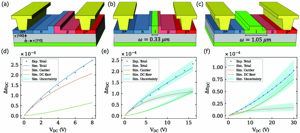
Fig. 1. (a) Depiction of PN junction, (b) PIN with intrinsic region width w = 0.33 μm w = 1.05 μm

Fig. 2. (a) Schematic view of the experimental setup used to measure the EOM from the MZM. DC voltage is applied to both arms; RF is either applied in single-drive or push–pull configuration (EDFA, erbium-doped fiber amplifier). (b) Effective index variations measured in push–pull configuration versus the reverse DC bias for a fixed RF peak amplitude of 1.4 V, (c) versus the RF amplitude for three reverse DC biases.
Fig. 3. Dots and the lines represent, respectively, the measurements and the corresponding fit or simulations. (a) Optical MZM transfer function for three electrical spectral components excluding intrinsic losses with P 0 P DC P Ω Ω P 2 Ω 2 Ω V DC = 6 V V RF = 2.0 V 2 Ω V RF Ω V DC Δ n 2 Ω Ω
Fig. 4. (a) Setup used to acquire eye diagrams (PPG, pulse pattern generator; DC, reverse DC bias; EDFA, erbium-doped fiber amplifier; DCA, digital communications analyzer). (b) Extinction ratio and signal-to-noise ratio at 10 Gbit/s by applying dual 4V p p DATA / DATA ‾
Fig. 5. Optical eye diagram display from 1 mm long PIN3 modulator by applying dual 2V p p DATA / DATA ‾ V DC = 30 V
Fig. 6. Optical transmission of an unbalanced MZI for an applied reverse bias of 0 and 30 V. λ r FSR ( λ r ) Δ λ r
Fig. 7. Measurements (dots) of P DC P Ω Ω P 2 Ω 2 Ω V DC = 2 V V RF = 0.51 V V DC = 4 V V RF = 1.6 V V DC = 6 V V RF = 2.0 V
Fig. 8. Eye diagram, respectively, measured at 2, 10, 18, 30 V reverse DC bias at 10 Gbits/s using 4V p p
Fig. 9. Optical eye diagram of 6 mm long PIN3 modulator measured at a data rate of (a) 32 Gbit/s and (b) 40 Gbit/s using 4V p p V DC = 30 V
Fig. 10. Cross section of the fabricated device viewed with an SEM.

Set citation alerts for the article
Please enter your email address
© Copyright 2018-2021 | Chinese Laser Press. All Rights Reserved 沪ICP备15018463号-20