
Jonathan Peltier, Weiwei Zhang, Leopold Virot, Christian Lafforgue, Lucas Deniel, Delphine Marris-Morini, Guy Aubin, Farah Amar, Denh Tran, Xingzhao Yan, Callum G. Littlejohns, Carlos Alonso-Ramos, Ke Li, David J. Thomson, Graham Reed, Laurent Vivien. High-speed silicon photonic electro-optic Kerr modulation[J]. Photonics Research, 2024, 12(1): 51
- Photonics Research
- Vol. 12, Issue 1, 51 (2024)
Abstract
1. INTRODUCTION
Integrated electro-optic (EO) modulators are a key component in systems such as classical and quantum optical communications, photonics-based quantum computing, and sensing. These systems target high-speed and low power consumption optical modulators. Silicon (Si) modulators, which rely primarily on the plasma dispersion effect [1], are intrinsically limited in speed due to their high RC constant [2]. Si modulators relying on the Pockels effect could overcome these limitations to produce a fast and pure phase modulation. Since silicon does not have a natural due to its centrosymmetric structure, such modulation cannot be achieved directly except by straining the crystal lattice [3] leading to a low resulting Pockels coefficient. The integration of high- materials on the Si platform has been widely considered. These include doped polymers, barium titanate (BTO) [4], lead zirconate titanate (PZT) [4], and lithium niobate (LN) [4]. These approaches require the development of hybrid or heterogeneous integration processes that increase the technology complexity. An EO modulation in Si can also be achieved through the DC Kerr effect that electrically induces an effective , which can be, hence, exploited to vary the refractive index by applying an electrical modulation superimposed to a static field. The DC Kerr effect has been studied in bulk silica [5], bulk silicon [6,7], silicon interface [8], bulk antiferromagnetic NiO [9], and in integrated platforms including silicon–organic hybrid [10], silicon-rich nitride [11], silicon rich carbide [12], and silicon nitride [13]. It has also been studied in the silicon platform for electric field-induced (EFI) second-harmonic generation (EFISHG) [14], EO modulation (EOM) [15,16], slow light regime [17], and cryogenic experiments [18]. However, the high-speed EOM in Refs. [15–17] using PN junctions led to a plasma dispersion effect that has a higher contribution to the modulation than the DC Kerr effect. While the DC Kerr effect has been well studied in the DC regime, no assessment discriminating the contribution of the DC Kerr effect and plasma dispersion modulation in the dynamic regime has been reported to our knowledge. This paper presents a comprehensive analysis of the DC Kerr effect induced in a PIN diode inserted in a silicon Mach–Zehnder interferometer (MZI) in both static and dynamic regimes. Data transmission has been analyzed up to 100 Gbit/s in non-return-to-zero (NRZ) format. An experimental method has been developed to assess the relative contribution of plasma dispersion from the Kerr effect in the dynamic regime.
The DC Kerr effect, also known as EFI Pockels effect, originates from the third-order nonlinear susceptibility tensor in presence of a static electric field. The refractive index change induced by the Kerr effect when a static electric field and an RF field are applied to the PIN junction is given by [10]
2. RESULTS AND DISCUSSION
Static and dynamic studies are conducted to distinguish Kerr effects from plasma dispersion on the index variation in three different unbalanced Mach–Zehnder modulators (MZMs). They consist of either PN or PIN junctions named PN, PIN2, PIN3, and their respective intrinsic region widths are , 0.33, and 1.05 μm (Fig. 1). Each junction waveguide has the same cross-sectional design with a 450 nm width, a 220 nm height, and a 100 nm slab thickness, suitable for the propagation of a single TE polarization mode (Appendix G, Fig. 10). The unbalancing of the MZMs is realized by a length difference between the arms leading to a passive phase shift with , the group index of our waveguide. The operating point of the MZM can, thus, be adjusted at the quadrature () without the need of heaters by only tuning the laser wavelength around 1550 nm.
Sign up for Photonics Research TOC. Get the latest issue of Photonics Research delivered right to you!Sign up now
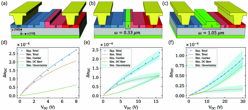
Figure 1.(a) Depiction of PN junction, (b) PIN with intrinsic region width
A. Measurement of the DC Kerr Modulation
The first experiments focus on the comparison between the three junctions in MZMs under a DC bias voltage only. The variation of the effective index of the guided mode () as a function of the reverse DC voltage () applied to the junction is obtained by measuring the shift of the resonance wavelength ,
B. Measurement of the EFI Linear EO Effect
The study of the EFI linear EO effect in the angular frequency modulation focuses on the PIN3 junction, which shows a dominant contribution of the DC Kerr effect in the effective index change (4 times greater than the contribution from plasma dispersion) as seen in Fig. 1(f). A common DC bias voltage is applied to both arms of the MZM and a sinusoidal RF signal () is split with two opposite phases to be applied in push–pull configuration. The optical wavelength is chosen to operate at the quadrature point. A simplified schematic view of the experimental setup to characterize the EOM is provided in Fig. 2(a). It is worthwhile to notice that the push–pull configuration of the MZM driving leads to assessing the index variation versus voltage as an equivalent efficiency of a single path because the measured index variation is twice the index variation in each arm while the considered voltage is twice of what is applied to each arm. The RF analysis in the push–pull configuration leads moreover to the cancellation of DC shift terms from Eq. (1) of the index variation in the MZM output measurements because the shift is the same in each arm.
![]()
Figure 2.(a) Schematic view of the experimental setup used to measure the EOM from the MZM. DC voltage is applied to both arms; RF is either applied in single-drive or push–pull configuration (EDFA, erbium-doped fiber amplifier). (b) Effective index variations measured in push–pull configuration versus the reverse DC bias for a fixed RF peak amplitude of 1.4 V, (c) versus the RF amplitude for three reverse DC biases.
The transfer function of the MZM as a function of the phase shift is
For a 6 mm long junction, a linear behavior of the effective index change as a function of the applied reverse DC bias and RF amplitude is observed in Figs. 2(b) and 2(c), respectively. This is a clear signature of the EFI linear EO effect. In Fig. 2(b), the non-zero intersection and nonlinear behavior of around indicates that carrier modulation is dominant relative to the EFI linear EO effect at low reverse DC voltages. The slope of the curve allows us to determine the coefficient (). See Appendices D and E for more information. This value is slightly underestimated (Appendix E) due to the carrier contribution having a negative evolution with . However, it remains relatively close to the values found in the literature.
C. Measurement of the Quadratic EO Effect
The quadratic EO effect at the angular frequency of can only be observed in a single-drive configuration, as it is proportional to the square of the electric field. We studied the transfer function at angular frequencies of and to separate the modulation behavior resulting from the distortion produced by the nonlinear transfer function of the MZM [Eq. (3)] and the quadratic EO effect. A bandpass RF filter centered at was placed at the signal generator output ensuring a very high rejection at . We considered the PIN3 junction where distortion due to the carrier absorption modulation is negligible.
The phase shift induced by the plasma dispersion and the Kerr effects can then be written as
The and components of the MZI spectral response can be written—after inserting the phase shift [Eq. (6)] in the MZM transfer function [Eq. (3)], performing a Jacobi–Anger expansion, and neglecting intermodulations—as follows:
The modulation indices and are determined by fitting the DC transmission and the spectral responses using Eqs. (8) and (9) at fixed reverse DC and RF voltages. See Appendix F.
The measurements performed for a 5 mm long PIN3 junction [Fig. 3(a)] show that the component is induced by the quadratic EO effect and not the signal distortion (the modulation operates at quadrature). Then, we can extract the corresponding modulation index from the response of the PIN3 junction. We can notice that it is, however, not possible to extract the modulation index from the responses of the PN and PIN2 junctions because the distortion induced by carriers is too important (see Appendix F, Fig. 7). The modulation indices and are accurately extracted at different reverse DC and RF bias voltages for the PIN3 junction using this method.
![]()
Figure 3.Dots and the lines represent, respectively, the measurements and the corresponding fit or simulations. (a) Optical MZM transfer function for three electrical spectral components excluding intrinsic losses with
Figure 3(b) shows the linear variation of the refractive index change as a function of the square RF voltage (i.e., quadratically increases with the RF voltage). This variation is independent of the applied reverse DC voltage, as expected with a quadratic EO effect. In addition, a linear fit of with respect to is performed to extract the coefficient (). This value is close to the average value from the literature and is consistent with the value found in the previous section.
Moreover, the measurements of the and components of the spectral response can be used to calculate the EFI linear EOM contribution to the modulation at using Eqs. (5) and (7),
The DC electric field inside the PIN junction is estimated using with the built-in voltage and the width of the intrinsic region [16]. See Appendix D. The RF field is estimated from the small signal approximation .
The contributions of the EFI linear EOM () and carrier modulation [] in the spectral response are reported in Fig. 3(c) showing that, above and at a modulation frequency of 5 GHz, the EFI linear EO effect contribution to the modulation becomes greater than the carrier modulation and reaches more than a factor of 3 at 15 V. A good agreement with simulations from Fig. 1(f) is obtained.
D. Eye Diagram Experiments
The data transmission characteristics of EO modulators based on the DC Kerr effect using PIN3 diode have been analyzed. The DATA and signals from an SHF bit pattern generator were amplified and transmitted to the respective arms of the MZM in push–pull configuration. A schematic view of the setup is shown in Fig. 4(a).
![]()
Figure 4.(a) Setup used to acquire eye diagrams (PPG, pulse pattern generator; DC, reverse DC bias; EDFA, erbium-doped fiber amplifier; DCA, digital communications analyzer). (b) Extinction ratio and signal-to-noise ratio at 10 Gbit/s by applying dual 4
First, optical eye diagrams were acquired at 10 Gbit/s on a digital communication analyzer (DCA) from a 6 mm long modulator with each arm driven at 4 and at different reverse DC bias voltages. The extinction ratio (ER) and the signal-to-noise ratio (SNR) of the modulated optical signal were computed by the DCA. The ER is greatly improved by reverse bias [Fig. 4(b)]. Indeed, for a varying from 2 to 30 V, the measured ER increases from 1.5 to 3.7 dB, and the SNR increases from 8.9 to 15.6. These results are entirely explainable with the EFI linear EO modulation behavior studied in Fig. 2. (More eye diagrams as a function of are presented in Appendix G, Fig. 8.)
At higher data rate, the DC Kerr effect improves the transmission capability, reaching a maximum data rate of 40 Gbit/s for the same 6 mm long PIN3 modulator with each arm driven at 4 [Appendix G Fig. 9(b)]. Its speed is limited by the RF electrode bandwidth, which can be further improved by redesigning the traveling wave electrodes to achieve an expected EO bandwidth of about 40 GHz for 1 cm propagation length [21].
Then, the bandwidth limitation of DC Kerr modulators for higher speed optical modulation was investigated on shorter modulators with 1 mm long PIN3 modulator with each arm driven at 2. The obtained speed limit shows a closing of the eye diagram around 80 Gbit/s [Fig. 5(a)] imputed to the limited traveling wave electrodes bandwidth, which is the same as the achieved speed limit of 1 mm long conventional depletion modulation under same test setup [22]. At 100 Gbit/s, the use of numerical six taps feed-forward equalization (FFE) has led to the open eye diagram [Fig. 5(b)] showing that such a DC Kerr modulator associated with the proper equalizing equipment could be promising to achieve very high speed modulation.
![]()
Figure 5.Optical eye diagram display from 1 mm long PIN3 modulator by applying dual 2
E. Prospect
The speed of silicon DC Kerr modulators can be improved by designing better traveling wave electrode or by removing the substrate to increase the electrode bandwidth by reducing the high-frequency electrode losses and the mismatch between the optical and RF group indices [23]. The doping level in PIN junctions does not limit their high-frequency response as their intrinsic RC bandwidth is greater due to the reduced loaded capacitance. Additionally, simulation results show the PIN modulator leads to a low doping-induced insertion loss of 0.11 dB/mm to be compared to about 1.5 dB/mm [24] for normal PN junction waveguides with . The for PIN phase shifter is estimated at for the current device working at 10 Gbit/s with 26–30. The low optical loss of PIN phase shifters at high reverse DC biases [25] allows to build high Q-factor silicon ring resonators based on the DC Kerr effect to improve frequency comb generation quality of ring modulators [26]. Such implementation of the DC Kerr ring modulator would reduce the footprint compared to MZI, and the speed limit will only be limited by the cavity quality factor. Because the maximum refractive index shift achievable using the DC Kerr effect is obtained when the electrical field inside the junction is maximum (close to the PIN junction avalanche) [27], a trade-off needs to be made among the high DC bias necessary to reach the maximum field, the carrier contribution, and the desired EO bandwidth limited by the RC constant, all increasing with the intrinsic region width [27]. Further improvements of the DC Kerr effect could be driven by optimizing the overlap between the optical and electric fields, i.e., the optical confinement in the waveguide and by carefully selecting the doping region to maximize the electric field location inside the waveguide.
3. CONCLUSION
The EFI Pockels effect (i.e., DC Kerr effect) has been observed in a Si PIN junction-based MZM. The refractive index variations as a function of both reverse DC bias voltage and RF amplitude have been measured in the dynamic regime showing a linear response with the DC bias voltage at a fixed RF amplitude. The refractive index modulations at angular frequencies and resulting from an applied RF signal at the angular frequency have been extracted to quantify the EFI linear EO effect contribution to the modulation. We have shown that the DC Kerr effect is the main reason for the high-speed modulation above 5 V DC bias voltages in comparison with plasma dispersion effect. Furthermore, optical modulation has been demonstrated up to 100 Gbit/s for a 1 mm long MZM. Silicon modulators based on the EFI linear EO modulation show promising characteristics for high-speed optical communications when using in short MZMs or in ring modulators. But they can also be used in quantum and LIDAR applications, where the low loss and efficiency characteristics are more important than the high-speed one, using longer phase shifters thanks to the low loss of PIN junctions and pure phase modulation of Kerr effect.
Acknowledgment
Acknowledgment. The authors acknowledge CORNERSTONE team of University of Southampton for the device fabrication. J. Peltier acknowledge Victor Turpaud for fruitful discussions, and Quentin Chateiller and Bruno Garbin for the development of the Python package Autolab used in his experiments. D. J. Thomson acknowledges funding from the Royal Society for his University Research Fellowship.
APPENDIX A: STATIC MEASUREMENT
Figure
![]()
Figure 6.Optical transmission of an unbalanced MZI for an applied reverse bias of 0 and 30 V.
APPENDIX B: EFFECTIVE INDEX AND CONFINEMENT FACTOR
The confinement factor of the TE mode needs to be considered to correctly estimate the experimental value of the coefficient.
Effective refractive index definition:
The confinement factor can be generally defined as
In the case of Kerr modulations, the refractive index becomes
By assuming a constant field inside the waveguide, the effective refractive index modulation becomes
Therefore, the effective modulation of the and components of the spectral response can be written as
APPENDIX C: EFFECTIVE LENGTH AND RF LOSSES
RF losses from our setup (RF filter, cables, splitter, a phase shifter, and RF probes) are measured to accurately estimate the values of the applied RF amplitude to the PIN junction. They are taken into account in for the corresponding output power displayed from the generator.
RF signal loss at the position z from the line is calculated using
The propagation losses of the RF line were extracted from RF transmissions at different line length. These losses need to be taken into account in the phase shift equation to define the effective lengths.
Phase variation equation:
The modulation index of the electric field-induced (EFI) linear electro-optic (EO) effect at the spectral component is calculated using Eqs. (
The effective length for this component is defined as
The modulation index of the quadratic EO effect at the component is calculated using Eqs. (
The effective length for this component is defined as
APPENDIX D: FIELD INSIDE THE JUNCTION
The DC electric field inside the PIN junction is estimated to be
For the PIN3 junction, the doping levels of boron () in the P region and of phosphorus () in the N region are . The intrinsic region has a Boron doping level of . is the relative permittivity of silicon, resulting in and .
The RF field is estimated from the small signal approximation,
APPENDIX E: DETERMINATION OF THE EFI LINEAR EO EFFECT
In the push–pull experiment, the amplitude of the EFI linear EO modulation (at component) is estimated from the slope of the DC sweep using Eq. (
For the PIN3 junction, the RF field variation with the DC field is small due to the small intrinsic region width variation with the applied DC bias and can be neglected (). The carrier variation is, however, not neglectable and is expected to be negative (), resulting in an underestimation of the coefficient using the slope of the measurement:
APPENDIX F: FITTING THE SPECTRAL COMPONENTS
The output DC optical power of the MZI and the and components of the spectral response are measured as a function of the wavelength for a fixed DC bias and RF modulation. Their respective noise is subtracted.
The expected components are
In the main paper, these equations are approximated assuming a small modulation index resulting in , , and .
First, we fit the static phase variation of the DC curve using Eq. (
Figure
![]()
Figure 7.Measurements (dots) of
APPENDIX G: EYE DIAGRAM EXPERIMENTS
Figure
![]()
Figure 8.Eye diagram, respectively, measured at 2, 10, 18, 30 V reverse DC bias at 10 Gbits/s using 4
![]()
Figure 9.Optical eye diagram of 6 mm long PIN3 modulator measured at a data rate of (a) 32 Gbit/s and (b) 40 Gbit/s using 4
APPENDIX H: SAMPLE FABRICATION
The silicon MZI modulators are fabricated through silicon photonics foundry CORNERSTONE [
![]()
Figure 10.Cross section of the fabricated device viewed with an SEM.
APPENDIX I: SETUP FOR DYNAMIC MEASUREMENTS
A T100S-HP tunable laser is used to inject light into the device via the grating couplers. A polarization controller is used to ensure a TE-mode injection. A 90/10 splitter is used to separate the output power; 10% goes into a CT400 optical components tester to measure the DC optical power, and 90% goes to a Keopsys KPS prebooster set to output a constant 3 dBm power. The amplified modulated optical signal is collected using a Agilent 83440D photodiode and fed to an Anritsu MS2830A signal analyzer set to monitor either the or components of the spectral response. A Keithley 2401 is used for polarized PIN junctions. The RF signals are generated using an Anritsu MG3694C signal generator. The signal is then coupled with the DC bias voltage using a Anritsu V251 bias-T. For push–pull experiments, the RF signal is split in half using an Anritsu V241C power splitter, and a phase delay is introduced on one arm using a Waka 02X0518-00 phase shifter. ACP 50 GHz GSGSG RF probes are used to apply the DC and RF bias voltages to the traveling wave electrodes. Measurements are done at the quadrature point by tuning the laser wavelength.
APPENDIX J: SETUP FOR EYE DIAGRAM MEASUREMENTS
MZI modulators are differentially driven with combined and by using two high-voltage bias tees (SHF BT45R – HV100). The high-speed signals are generated from an SHF bit pattern generator and amplified to 4 on each arm for modulation rates below 50 Gbit/s and to 2 for higher modulation rates up to 100 Gbit/s. NRZ signals are sent to the MZI modulators via 67 GHz GSGSG probes and terminated with DC blocks and 50 mΩ resistors. Measurements are done at the quadrature point. Eye diagrams are displayed using the averaging function of the DCA to reduce optical noise from EDFA.
References
[22] K. Li, D. Thomson, S. Liu. 112G baud sub pJ/bit integrated CMOS-silicon photonics transmitter. Research Square, PPR540568(2022).
[25] H. Rong, A. Liu, R. Jones. An all-silicon Raman laser. Nature, 433, 292-294(2005).
[27] C. G. Bottenfield, V. A. Thomas, S. E. Ralph. DC Kerr effect and limits for silicon photonic modulators. Conference on Lasers and Electro-Optics (CLEO), JTh2A.65(2019).

Set citation alerts for the article
Please enter your email address
© Copyright 2018-2021 | Chinese Laser Press. All Rights Reserved 沪ICP备15018463号-20