State Key Laboratory of Tunable Laser Technology, Ministry of Industry and Information Technology, Key Laboratory of Micro-Nano Optoelectronic Information System, Shenzhen Graduate School, Harbin Institute of Technology, Shenzhen 518055, China
Magnetic dipole (MD) transitions are important for a range of technologies from quantum light sources and displays to lasers and bio-probes. However, the typical MD transitions are much weaker than their electric counterparts and are usually neglected in practical applications. Herein, we experimentally demonstrate that the MD transitions can be significantly enhanced by the well-developed magnetic metamaterials in the visible optical range. The magnetic metamaterials consist of silver nanostrips and a thick silver film, which are separated with an :polymethyl methacrylate (PMMA) film. By controlling the thickness of the :PMMA film, the magnetic resonance has been tuned to match the emission wavelength of MDs. Consequently, the intensity of MD emission has been significantly increased by around 30 times at the magnetic resonance wavelength, whereas the intensity of electric dipole emission is well-preserved. The corresponding numerical calculations reveal that the enhancement is directly generated by the magnetic resonance, which strongly increases the magnetic local density of states around the MD emitter and can efficiently radiate the MD emission into the far field. This is the first demonstration, to the best of our knowledge, that MD transitions can be improved by an additional degree of magnetic freedom, and we believe this research shall pave a new route towards bright magnetic emitters and their potential applications.
When the initial state has not been significantly depleted by scattering to the final state , the decay rate of an emitter can be described with Fermi’s golden rule[1], where and are the angular frequencies of states and , and is the interaction Hamiltonian that can be expressed as
The first two terms on the right side of Eq. (2) represent the interaction of electric dipole (ED, ) and magnetic dipole (MD, ) with the environmental electric and magnetic field, respectively. The higher order interactions are neglected. By considering the intrinsic emitter properties and the influence of the environment, Eq. (1) can thus be rewritten as
From Eq. (3), it is very clear that the radiation rate of ED and MD can be significantly affected by the electric local density of states (LDOS, ) and magnetic LDOS (), which are the number of continuum states per unit of energy, and can be tailored by the photonic structures. Given the fact that MD transitions are orders of magnitude weaker than ED transitions, the control of ED emission has been thoroughly studied in different nanostructures[2–10]. Few studies have investigated the ways to control the MD emissions[11–20], which are recently recognized to be important for the magnetic light–matter interaction and the corresponding applications in magnetic mapping or sensing. In past few years, photoluminescence (PL) that is dominated with MD transitions has been reported by changing the crystal symmetry of the environmental matrix[21]. Very recently, Karaveli and Zia have experimentally demonstrated the MD emission dominated PL by suppressing ED transitions with electric resonances in nanostructures or cavities[12]. However, the direct enhancement of MD transitions in the experiment, which has been considered a milestone in the development of a bright magnetic emitter, is still rarely studied[17].
Sign up for Chinese Optics Letters TOC. Get the latest issue of Chinese Optics Letters delivered right to you!Sign up now
To control the MD transitions, the most straightforward and efficient way is tailoring the magnetic LDOS around the MD emitters [see Eq. (3)][1]. From this point of view, magnetic metamaterials can be very promising candidates[22–26]. In principle, metamaterials can process strong magnetic response in the optical wavelength range and, thus, dramatically modify the magnetic LDOS (). As a result, controlling MD emission with metamaterials has quickly gained considerable research attention in the past decade. In 2010, Feng et al. theoretically demonstrated a 360 times enhancement by placing the MD at the magnetic hot spot of the coupled square-patches-based metamaterials[11]. Soon after, Rolly et al. theoretically proposed that the magnetic resonances of silicon particles can enhance the MD emission of trivalent erbium ions by around 90 times[14]. A similar idea has also been theoretically demonstrated within the magnetic metamaterials that are composed of coupled nanostrips or split rings[27]. However, up to now, most of the researches are restricted in theoretical studies, and the experimental demonstration is hindered by the difficulty in placing MD emitters into the spacer between coupled nanostrips. While plasmonic nanoholes or split rings can realize magnetic resonance with a single layer, they are either working at a long wavelength of around 2 μm or coupled to dark magnetic modes. Although Choi et al. have reported plasmonic enhancement of MD emission for ions at 1.5 μm, the complex PL band deeply mixing ED and MD states makes it impossible to enhance the ED and MD emissions separately[28]. In the latter case, the enhanced MD emissions are mostly dissipated by the metallic nanostructures and hard to be observed in the far field. In this Letter, we fabricated a new and simple type of magnetic metamaterials and experimentally demonstrated the enhancement of MD transitions with magnetic resonances.
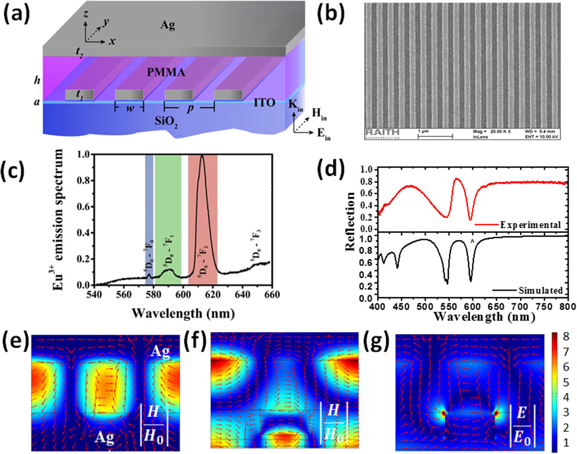
Figure 1(a) depicts the schematic picture of the designed nanostructure. It consists of a one-dimensional periodic Ag nanostrip array and a thick Ag film, which are separated by a polymethyl methacrylate (PMMA) spacer. The thicknesses of the nanostrip, Ag film, and PMMA spacer are , , and , respectively. In principle, the PMMA coated nanostrips can support a plasmonic mode with a single reflection deeply dependent on the periodicity () and width (). These phenomena are very regular in plasmonic devices. When a thick Ag film is coated on top of the PMMA film, the spectrum dramatically changes. The plasmonic modes in Ag nanostrips have their mirror images in the Ag mirror, and they can interact with the images. Since the mirror images always have reserved phases, here, only the anti-symmetric current flow can be generated in the upper metal film and the bottom nanostrips. Thus, a strong magnetic field is formed within the PMMA spacer, where the active media can be easily embedded.
Figure 1.(a) Schematic picture of the hybrid plasmonic system with Ag nanostrip arrays and Ag film sandwiched by an :PMMA layer. (b) The scanning electron microscope (SEM) image of the nanostrip structure before being coated with the :PMMA layer. (c) Emission spectrum for :PMMA film recorded under 385 nm excitation. (d) Experimentally measured (red line) and numerically calculated (black line) linear reflection spectra of the sample for TM polarizations. (e) The distribution of the magnetic field enhancement factor at 595 nm. (f) The distribution of the magnetic field enhancement factor at 545 nm. (g) The distribution of the electric field enhancement factor at 610 nm.
Based on above analysis, we have designed the hybrid nanostrip-film system and numerically studied the enhancement of ED and MD transitions. The geometry parameters of Ag nanostrips are the period , the thickness , and the width . The thicknesses of the indium-tin-oxide (ITO) film, PMMA film, and Ag film are , , and , respectively. The reflection spectrum of the designed nanostructure is numerically calculated by using the finite-element method (COMSOL Multiphysics). The optical property of Ag is directly taken from the experimental results by considering additional loss from the scattering of the nanostructure edge. The numerical result is plotted in the top panel of Fig. 1(d), where two resonant dips at 595 and 545 nm can be clearly seen. The normalized magnetic field distribution of resonance at 595 nm is plotted in Fig. 1(e). The magnetic field is highly localized inside the PMMA spacer, and the maximum intensity enhancement factors exceed 80 at 595 nm. The average field intensity enhancement factor (Purcell factor) of 35 is obtained by averaging the field intensity enhancement factor among the :PMMA region. Similar results have also been obtained from the resonance at 545 nm [see Fig. 1(f)]. However, due to the hybridization of magnetic resonance and plasmonic mode, here, the ratio of the magnetic field within the PMMA film is a little bit smaller, and the average enhancement factor is around 6 at 545 nm. For a direct comparison, the electric field distribution at 610 nm has also been calculated [see Fig. 1(g)]. Because no resonance occurs at this wavelength, the electric field is only slightly modified, and the corresponding average electric field enhancement factor (Purcell factor) is about 13.7 among the :PMMA region.
Following Eq. (3), it is very easy to see that the decay rate can be significantly influenced by the enhanced magnetic field. In case that the MD emitter is placed within the PMMA film at the position of with transition frequency , the magnetic LDOS () can be expressed via where is the unit vector in the MD direction, and is the magnetic Green function. Then, the enhancement factor of MD transitions can be numerically calculated. For practical applications as a magnetic emitter, the enhancement of the MD emission in the far field is more important. Here, we define the radiative emission enhancement factor (RE) as a measure to characterize the MD emission change in the far field domain. For the structure with power loss, the total decay rate () is usually divided into radiative decay rate () and nonradiative decay rate (). Thus, RE can be expressed as
Here, is the power recorded in the far field, and is the power in free space without the hybrid structure. When a single MD emitter is placed at the arbitrary position inside the PMMA film (for example, in the center “O” point, as seen in the insert in Fig. 2) with the dipole moment direction along axis and parallel to the strips, the enhancement factor can be numerically calculated by integrating the outflowing energy along the axis in the far field with and without structure. Taking the orientation into consideration, the general radiative enhancement for random orientation dipoles is the average value of the radiative enhancement of MDs with their dipole moment parallel to the , , and axes, respectively. The red line in Fig. 2 shows the average RE for MDs as a function of the wavelength under consideration of random orientation of dipoles. The average RE is obtained by averaging the RE values for 250 dipoles located uniformly inside the PMMA layer. The average RE for MD stays above 1 from 560 to 660 nm and reaches the peak value at 595 nm, which is near the MD emission wavelength of [see Fig. 1(c)] at 590 nm, demonstrating that the hybrid structure can modulate the emission using magnetic LDOS. Similarly, ED emitters are placed at the same positions to calculate the RE. The average result is plotted as the black line in Fig. 2. Due to the nature of the designed magnetic nanostructure, here, the RE for ED transitions also has a peak around 595 nm and declines quickly away from the resonance. However, the structure still works as a reflective metallic mirror and the RE for EDs at 610 nm stays above 3.6. Therefore, based on the enhancement in ED and MD transitions, we can conclude that the proposed hybrid nanostrip-film structure is especially suitable to be a magnetic nanoantenna, which can couple with and enhance the ED and MD emitter well at the same time.
Figure 2.Enhancement factor for power transferred into the far field from an MD emitter and an ED emitter placed in the center of the hybrid system. The result is averaged over all possible orientations of the emitter and normalized to the power emitted in vacuum. We observed large enhancement of more than 1 order of magnitude at the resonance for the MD emitter centered around 595 nm.
We then fabricated the hybrid nanostrip-film structure and studied its influences on MD emissions. Basically, the geometry of the sample was first defined by an electron beam (E-beam) writer on a glass substrate with a 15 nm thick ITO layer. Then, standard E-beam deposition followed by lift-off was used to produce an Ag nanostrips array. Note that a 10 nm alumina layer was added to the bottom of the Ag strips to improve the fabrication stability. The final nanostrip array is in size, and the high resolution field emission scanning electron microscope (FE-SEM) image is shown in Fig. 1(b). All the geometrical parameters match the design well. Then, a PMMA layer embedded with Eu m (III) hexaflouroacetylacetonate [, Sigma Aldrich, 18.8% in weight] was spin-coated onto the top of the nanostrip followed by E-beam deposition of another Ag layer. In the current experiment, the thickness of the PMMA film is , and the top surface is almost flat under an atomic force microscope. Thus, the final experimental structure is quite similar to the initial design.
The fabricated hybrid nanostrips structure was optically characterized using a homebuilt reflection setup with light incident from the glass side. The measured reflection spectrum for TM polarized incident light is displayed as the bottom panel in Fig. 1(d). The reflection spectrum exhibits two distinct dips at 592 and 545 nm. The resonant wavelengths, full width at half-maximum (FWHM), and depths of the mode at 592 nm match the numerical calculation very well, clearly indicating its nature of magnetic resonance. The other dip at 545 nm results from the strong coupling between the magnetic resonance and the surface plasmonic resonance. Considering the emitters in the current design, it has prominent magnetic emission at 590 nm [see Fig. 1(c)], which is close to the magnetic resonance, and, thus, it is possibly significantly enhanced. Meanwhile, it also has an ED emission at 610 nm that can be used for a direct comparison.
Then, the sample was excited by a femtosecond Ti:sapphire laser (1 kHz, 100 fs duration) at a wavelength of 385 nm under a homemade microscope system. The PL was collected by the same objective lens () and recorded by a CCD coupled spectrometer. The sample was excited by a laser with two types of polarizations, which have an electric field parallel (TE polarization) and perpendicular (TM polarization) to the nanostrips, respectively. A polarizer was placed in front of the collection fiber to detect the polarization of the PL. The polarizers at 0° and 90° correspond to the TE and TM polarizations as defined above. Figure 3 shows the emission spectra of under different conditions. Here, the exciting laser is TM polarized, and the same results have been achieved with a TE polarized pumping laser (see Fig. 3). Although the thickness of the PMMA film and the density of are identical in all samples, the intensities of the emission spectra vary significantly with the change of nanostructure. The green and cyan solid lines in Fig. 3 are the reference TE and TM polarized PL of PMMA: film on a glass substrate. The well-known emission peaks at 610 nm (ED emission) and 590 nm (MD emission) can be seen, and the difference between TE and TM polarizations is negligibly small. When the PMMA: film is spin-coated onto a 55 nm Ag film, the cases are a little bit different. The ED emission at 610 nm is enhanced by about 3.3 times. On the contrary, no obvious enhancement can be observed for MD emission. This is because the conventional plasmonic structure mostly affects the ED transitions instead of MD transitions. When the thickness of the PMMA film was increased to several hundred nanometers, the MD emission was possibly dominant of the PL, but it was still caused by the suppression of ED transitions, according to previous reports.
Figure 3.Emission spectra of the ions embedded in the hybrid nanostructure with TM and TE polarizations (blue and purple lines), the 55 nm thick Ag film with TM and TE polarizations (black and red lines), and the bare glass substrate with TM and TE polarizations (green and cyan lines). The spectra are normalized to the maximum of the ED emission at 610 nm of the embedded in the hybrid nanostructure.
Once the PMMA: film is embedded between the Ag nanostrips and the thick Ag film, the emission spectra are totally different. The purple line and blue line in Fig. 3 are the recorded TE polarized and TM polarized PL spectra. Compared with the reference PL at 610 nm, both of the TE and TM polarized PL is enhanced by factor of 4, which is about 1.2 times higher than that for on top of the Ag layer. The most interesting phenomenon happens at the MD emission, which is centered at 590 nm. For the TE polarized PL, the MD emission at 590 nm still has similar intensity to the reference PL. In case of TM polarization, the MD emission at 590 nm is much stronger than the reference PL through the wavelength from 583 to 603 nm. The different enhancement efforts are consistent with our above analysis and numerical calculation. As illustrated in Fig. 1(d), no resonance can be observed at 610 nm for both of TE and TM polarizations. Then, the hybrid structure works mostly like a metallic surface. As a result, the ED emission enhancement factors at 610 nm for both TE and TM polarizations are similar to the case of PMMA: on top of the thick Ag film. Contrarily, the hybrid structure processes a strong magnetic response at 595 nm for the TM polarization. As discussed above, the magnetic resonance can strongly enhance the magnetic LDOS and thus affect the magnetic decay rate and the corresponding RE factor.
To further confirm the contribution of magnetic resonance, we have carefully studied the MD emission in the far field as a function of emission polarization. All the results are summarized in Fig. 4(a). With the increase of the polarization angle from 0° (TE) to 90° (TM), we can see that the MD emission is gradually enhanced. The PL intensity is normalized to the PL intensity for TE polarization and plotted in Fig. 4(b). The normalized PL intensity keeps increasing from 1 to 5, and the change fits the polarization equation well [see Fig. 4(b)]. Thus, we can confirm that only TM polarized magnetic resonance mainly contributes to the final RE factor. Figure 4(c) summarizes MD emission spectra from MDs embedded in the hybrid structure and in a pure film with TM polarization as a function of wavelength. Once again, we can see that the emission is highly enhanced, and an enhancement factor of 31 is achieved at 595 nm, which matches very well with the simulated result. When the wavelength deviates from 595 nm, the enhancement in the magnetic field gradually decreases and finally disappears. At the same time, the enhancement factor for ED emission at 610 nm is about 4, which is also very close to the simulated result in Fig. 2. The results confirm that the proposed hybrid metamaterial can modulate the electric and magnetic LDOS at the same time. As a result, both of the ED and MD emissions that form can be effectively enhanced.
Figure 4.(a) The fitting spectra for MD emission with TE polarization with 0° to TM polarization with 90°. (b) The PL emission intensity for MD emission via the polarization. The PL intensity is integrated following the equation . (c) The enhanced PL spectra of the ions embedded inside the hybrid structure with magnetic LDOS with TM polarization in the red line. For comparison, the PL spectrum from :PMMA with the same polarization is also shown with the black line, enlarged 10 times for clarity. The net PL enhancement was evaluated by normalizing the excitation power incident into the structure.
In conclusion, direct enhancement of MD has been theoretically proposed and experimentally realized in a hybrid plasmonic structure. The hybrid system processes bright magnetic resonance, which can enhance the MD transitions as well as radiating the MD emission to the far field. As a result, the experimentally recorded MD emission of has been enhanced by a factor of 31, which is the record high value for the direct enhancement of MD. This research presents an important step toward using engineered metamaterials to obtain bright MD emitters at optical frequencies, and it shall also pave a new route for practical applications in magnetic quantum light sources, lasers, and magnetic bio-probes.
References
[1] L. Novotny, B. Hecht. Principles of Nano-Optics, 271(2011).