
Chuan Shen, Sui Wei, Haixiu Yu, Bo Tao. Model of Liquid Crystal on Silicon Device with Sub-Wavelength Grating Structure[J]. Acta Optica Sinica, 2020, 40(3): 0305001
- Acta Optica Sinica
- Vol. 40, Issue 3, 0305001 (2020)
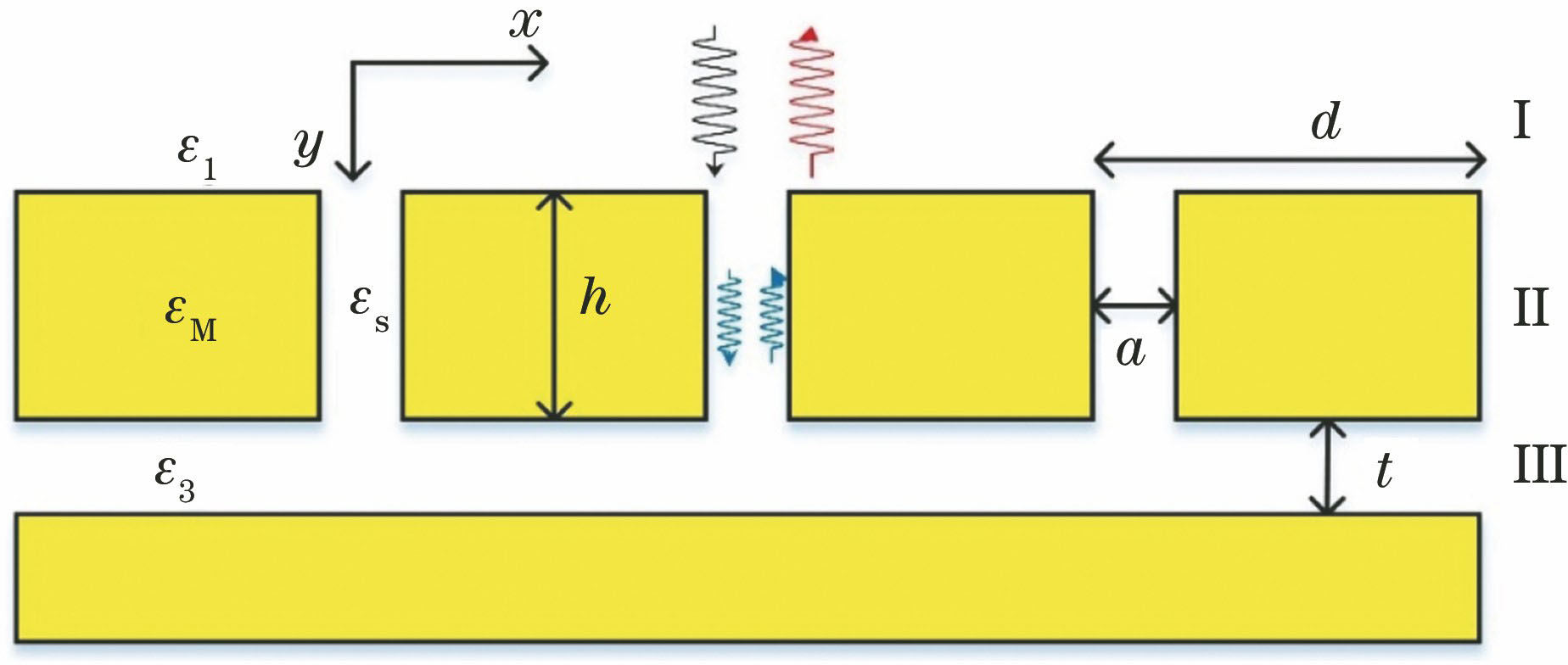
Fig. 1. Schematic of GLCoS structure
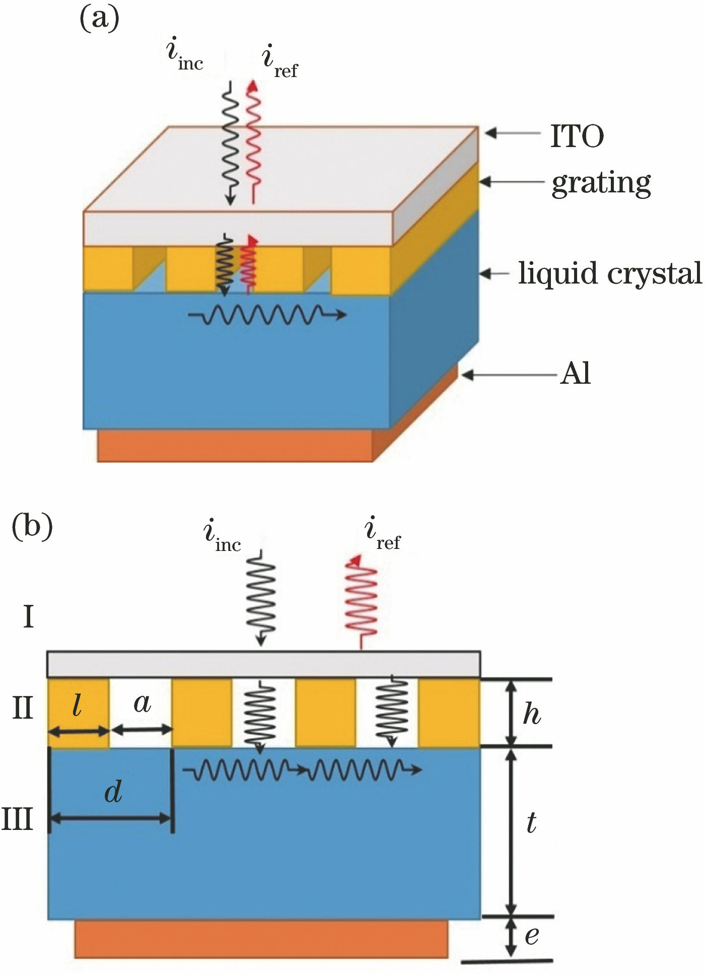
Fig. 2. Structural design drawing of GLCoS. (a) Stereo structure of proposed model; (b) cross-sectional schematic of structure
Fig. 3. Overall flow chart of simulation
Fig. 4. Phase modulation curves with different slit numbers
Fig. 5. FP resonance at different depths of metal gratings. (a) Grating height of 80 nm; (b) grating height of 100 nm; (c) grating height of 130 nm; (d) grating height of 150 nm
Fig. 6. Influence of thickness of intermediate layer on phase in visible light range
Fig. 7. Influences of different pixel gaps. (a) Phase modulation variation of reflected light; (b) amplitude variation of reflected light
Fig. 8. Influences of grating height and width. (a) Phase modulation variation of reflected light; (b) amplitude variation of reflected light
Fig. 9. Distributions of direction vector and electric field under different pixel gaps. (a) 260 nm; (b) 280 nm; (c) 300 nm; (d) 320 nm; (e) 340 nm
Fig. 10. Device structure. (a) Schematic of device; (b) local grating SEM image
Fig. 11. Schematic of experimental setup
Fig. 12. Results of processing. (a) Interferometric fringes; (b) results of filtering
Fig. 13. Reflection phase as a function of voltage. (a) Micro-nano structure part; (b) liquid-crystal part
|
Table 1. Parameters of GLCoS structure

Set citation alerts for the article
Please enter your email address
© Copyright 2018-2021 | Chinese Laser Press. All Rights Reserved 沪ICP备15018463号-20