
Dong-Pyo Han, Motoaki Iwaya, Tetsuya Takeuchi, Satoshi Kamiyama, Isamu Akasaki. Space-charge effect on photogenerated-current and -voltage in III-nitride optoelectronic semiconductors[J]. Photonics Research, 2021, 9(9): 1820
- Photonics Research
- Vol. 9, Issue 9, 1820 (2021)
Abstract
1. INTRODUCTION
Energy conversion is one of the primary functions of semiconductor devices. For example, light-emitting diodes (LEDs) and solar cells (SCs) are optoelectronic devices that functionally aim to convert energy from electricity to radiation and vice versa [1,2]. In principle, photons are generated via a bimolecular radiative recombination () process of injected charge carriers when an external bias with energy greater than the bandgap is applied to the semiconductor. In this case, the generated photon energy typically corresponds to the bandgap energy [3,4]. Inversely, charge carriers are generated when photons with energy greater than the bandgap are incident in a semiconductor device. With generated charge carriers, a photogenerated current () and photogenerated voltage () can be induced, thereby supplying electricity in an external circuit [5,6].
In energy conversion semiconductors, the identification of the conduction mechanism is of primary importance, as it plays a key role in determining a performance of the device. In other words, carrier recombination/generation processes are physically closely related to carrier conduction/transport processes [7,8]. Particularly, a discrepancy between the rate of carrier recombination and injection during electrical operation can introduce uncompensated space charges, causing that the concomitant push-back electrostatic field gives rise to space-charge-limited current (SCLC). In this situation, electrical driving currents are expected to exhibit a quadratic dependence on the voltage in defect-free semiconductors, which was first theoretically predicted by Mott and Gurney [9,10]. By developing the Mott–Gurney theory, Goodman and Rose theoretically predicted the occurrence of fundamental push-back electrostatic-limited conduction even during optical operation due to the unbalanced transport and buildup of charge carriers, which gives rise to space-charge-limited photocurrent in defect-free semiconductors [11,12]. To date, theories of the space-charge effect (SCE) are frequently adopted in an attempt to elucidate the conduction mechanism in organic optoelectronic semiconductors. In short, the physical mechanisms of the super-/sublinear dependence on the applied voltage () of the net current () in organic LEDs and SCs were elucidated by employing the abovementioned theories in several research papers [13–17]. However, only several studies have examined the SCE on the conduction of inorganic optoelectronic semiconductors.
Modern optoelectronic devices require high reliability, a long lifetime, and high mechanical strength. For this reason, inorganic semiconductors are currently attracting great attention. The most representative inorganic semiconductor is the III-nitride semiconductor, which is widely used in optoelectronics in the visible and ultraviolet (UV) spectral range owing to its inherent feature of a wide bandgap [18]. III-nitride semiconductors are already commercially available thanks to the first development of a high-quality p-type GaN by Akasaki
Sign up for Photonics Research TOC. Get the latest issue of Photonics Research delivered right to you!Sign up now
A heterojunction, the most widely adopted multiple-quantum-well (MQW) structure, is typically used as an active layer in inorganic optoelectronic semiconductors, which was first demonstrated by Alferov
In this study, we attempted to elucidate the SCE on and in AlGaInN-based optoelectronic semiconductors. To this end, we carefully investigated and analyzed photoexcited curves depending on the external quasiresonant optical excitation power at RT and cryogenic temperature (CT). It should be noted that Shockley–Read–Hall recombination () via defect levels in the MQWs is the main nonradiative process, which is inactive at CT due to the nature of freezing out [33,34]. That is, a further decrease in the total recombination rate in MQWs is expected, which accelerates the discrepancy [22]. Thus, investigation at CT is believed to be useful for this study because we expect the accelerated buildup of charge carriers in an artificially created defect-free device; that is, SCE-dominated conduction is predicted at CT. On the basis of the experimental results and analysis, we attempted to experimentally exhibit the SCE on and and to unveil the mechanism behind the phenomenon. We also discussed the SCE on the energy conversion efficiency of devices in detail.
2. EXPERIMENTAL DETAILS
For the experiments, an AlGaInN-based junction semiconductor device was prepared, and its structure was conventional. The sample was grown on a -plane patterned sapphire substrate by metalorganic vapor-phase epitaxy (Taiyo Nippon Sanso Co., EMC) equipped with 2-inch (∼5.1 cm) susceptors. From the sapphire substrate, the structure consisted of a 30 nm thick LT-GaN buffer layer grown at 480°C, a 3 μm thick undoped GaN layer grown at 1070°C as a template layer, and a 2.2 μm thick Si-doped layer grown at 1070°C as an n-type layer. Twelve pairs of (2 nm)/GaN (2 nm) superlattice layers and a 10 nm thick undoped GaN spacer layer (grown at 800°C) were sequentially grown on the n-type layer as a stress relief and defect capture layer [35,36]. As an active layer, five pairs of (3 nm)/GaN (10 nm) MQWs (grown at 780°C) were grown on the spacer layer. The bandgap energy of the MQWs was () at 300 K. Note that the MQWs were intentionally undoped (i.e., an intrinsic layer). Following this, a Mg-doped p-type GaN layer (150 nm) and a heavily Mg-doped -GaN contact layer (20 nm) were sequentially grown on the MQWs. A 60 nm thick indium-tin-oxide film was deposited by a radio frequency (RF) sputter system (Shibaura Mechatronics Co., CFS-4EP) on the -GaN contact layer. The sample was fabricated on chips with lateral electrodes (chip ) and packaged as surface mount devices. The curves were measured using a Keithley 2602 SourceMeter. A 405 nm continuous-wave laser (Coherent Inc., CUBE 405-100C) was adopted as the external optical pumping source for quasiresonant optical excitation. We controlled the spot size of the incident light to meet the sample size using a focusing lens. The electroluminescence (EL) and photoluminescence (PL) spectra were collected using a spectrometer (Avantes Co., AvaSpec-ULS2048). All measurements were performed in a closed-cycle cryostat (Advanced Research System Co., DMX-1AL) to maintain and control the operating temperature.
3. EXPERIMENTAL RESULTS, ANALYSIS, AND DISCUSSION
Figure 1(a) depicts the curves with quasiresonant optical excitation depending on the optical excitation power (0 to 100 mW) at RT, that is, excitation-power-dependent (PDIV) curves at 300 K. Notably, at 0 V (i.e., in the short-circuit condition) is defined as the short-circuit current (), which is denoted as squares herein. Figure 1(b) presents the magnified graph of Fig. 1(a), in which the open-circuit voltage () is denoted as circles, which is defined by at 0 A (i.e., in the open-circuit condition). It appears that both and increase with the increase in excitation power, indicating that the output electricity (i.e., ) increases with the increase in input optical power. These are typical characteristic of the PDIV in junction optoelectronic semiconductors, such as LEDs and SCs, in that the output power increases as the input power increases [37,38].
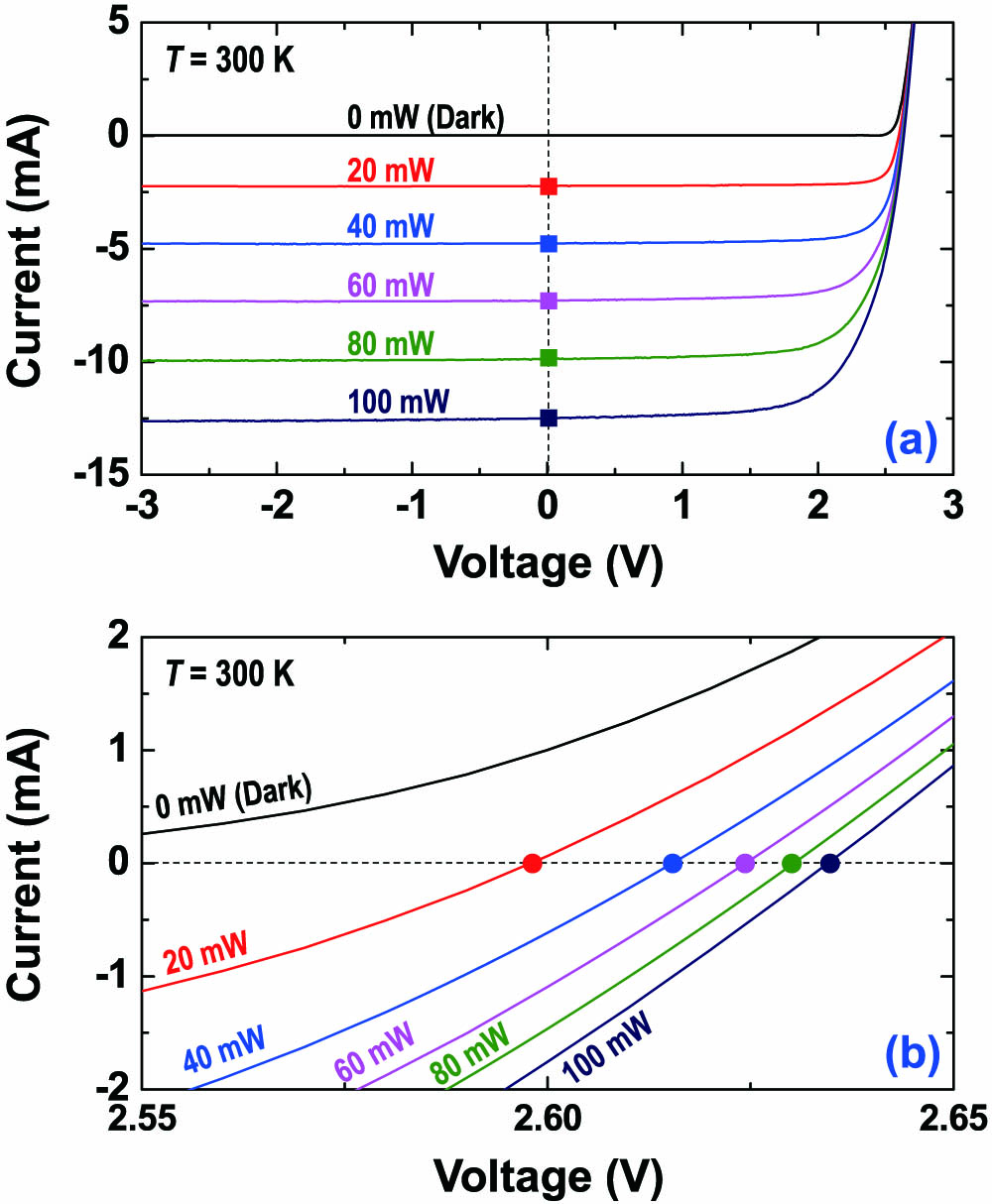
Figure 1.(a) Excitation-power-dependent
and can be plotted as functions of optical excitation power using the experimental results in Figs. 1(a) and 1(b), which are depicted in Fig. 2(a). We can observe different excitation-power-dependent behavior between them; that is, increases almost linearly, whereas increases rapidly in a low-excitation regime and then slowly increases.
![]()
Figure 2.(a)
Typically, the PDIV curve can be described in terms of the Shockley diode equation and as shown below [5,6,37]:
Next, we repeated the measurement of the PDIV curves in the same manner as in Fig. 1(a) at CT. Figure 3(a) presents the PDIV curves at 15 K (0 to 25 mW), in which is denoted as squares. Likewise, increases with increasing optical excitation power, while its absolute values are small compared to those at 300 K. Figure 3(b) presents the magnified graph of Fig. 3(a), in which is denoted as circles. Perhaps somewhat surprisingly, appears to no longer be independent of , and appears to decrease with increasing optical excitation power. Obviously, this PDIV behavior is abnormal because the output photogenerated electrical potential energy decreases, although the input incident power increases. The PDIV curves and its magnified graph at 15 K plotted for the same optical excitation power in Fig. 1 (0 to 100 mW) are displayed in Appendix A. Apparently, this phenomenon has a negative effect on device performance, especially in terms of energy conversion efficiency. Therefore, clarifying the mechanisms behind this phenomenon should be of primary importance in improving device performance.
![]()
Figure 3.(a) PDIV curves at 15 K and (b) magnified graph. Squares and circles denote
To examine this phenomenon more closely, and at 15 K are plotted as functions of excitation power in Fig. 4(a). Figure 4(a) indicates that as the optical excitation power increases, monotonically increases, while rapidly decreases and then saturates. The curve is plotted in Fig. 4(b) on a semi-log scale using the data in Fig. 4(a), and the curve with 0 mW at 15 K is included. The two curves have completely different shapes, and no point of contact or intersection is found. This result indicates that the PDIV curves at 15 K can no longer be described by the conventional Shockley diode equation in Eq. (1), and more complex phenomena seem to be involved.
![]()
Figure 4.(a)
To investigate and clarify the mechanism behind the abnormal behavior of PDIV at 15 K, we compared the EL and PL spectra at RT and CT. The analysis of emission spectra is useful, as it makes it possible to examine the energy distribution of charge carriers in MQWs; that is, the energy distribution of emitted photons corresponds to the carrier distribution in the allowed band of the MQWs [4,7,38]. Figure 5(a) displays the experimental results of the normalized PL spectrum at 80 mW in the open-circuit condition, the normalized EL spectrum at (), and the normalized EL spectrum at () at 300 K. Note that and at an excitation power of 80 mW are 10.1 mA and 2.63 V, respectively, at 300 K [refer to Fig. 2(a)]. We can observe an almost perfectly matched shape between PL and EL spectra when equals . However, they exhibit significantly different shapes when is equal to with not equal to . The result in Fig. 5(a) implies that the charge carrier density and the distribution of the charge carriers in the MQWs are almost the same when equals at 300 K; namely, an almost identical state of the allowed energy band and carrier distribution is expected when the carrier density in the MQWs is same. Again, the curve suffers from [see Eq. (2)]; thus, the state of the allowed band and carrier distribution is different when equals . In the same manner as Fig. 5(a), we measured the EL and PL spectra at CT. Figure 5(b) displays the experimental results of the normalized PL spectrum at 80 mW, the normalized EL spectrum at (), and the normalized EL spectrum at () at 15 K. Note that and at an excitation power of 80 mW are 1.9 mA and 2.55 V, respectively, at 15 K [refer to Fig. 4(a)]. Unlike the results at 300 K in Fig. 5(a), the spectra exhibit significantly different shapes even when equals . Note that the EL spectrum has a longer wavelength than the PL spectrum, which implies that the charge carriers distribute a higher energy state in the open-circuit condition at 80 mW than at . More detailed experimental results of EL and PL spectra are shown in Appendix B.
![]()
Figure 5.Normalized photoluminescence (PL) and electroluminescence (EL) spectra measured at (a) 80 mW, 10.1 mA (2.78 V), and 2.63 V (1.9 mA) at an operating temperature of 300 K and (b) 80 mW, 50 mA (4.23 V), and 1.9 mA (3.89 V) at 15 K, respectively.
In AlGaInN-based semiconductors, the EL and PL spectra typically exhibit blueshift characteristics with the increase in carrier density in MQWs. In other words, the charge carriers distribute a higher energy state in the allowed band of MQWs as the carrier density increases due to the simultaneous effect of the QCSE and PSF [44,45]. Concerning such blueshift characteristics, the carrier density in the MQW in the open-circuit condition at an excitation power of 80 mW should be greater than that at (i.e., ). To identify the same state of the allowed band with PL at 80 mW, we increased the driving current further. As depicted in Fig. 5(b), we were able to identify the EL spectrum with the same peak wavelength at a much higher driving current (50 mA) than . However, the shapes of the spectra were very different despite the same peak wavelengths, implying that the state of the allowed band in MQWs is completely different for the two operating conditions. Overall, we can infer that, unlike at 300 K, the carrier density in MQWs at 15 K is effectively higher than the prediction, which is believed to have a significant impact on the PDIV characteristics at 15 K.
In an attempt to elucidate the mechanism of the unexpected PDIV and emission spectra characteristics at 15 K, we proposed the carrier dynamics model, including the transport, accumulation, recombination, and generation process, which is schematically illustrated in Figs. 6(a) and (b). Note that only electrons are considered in this model, as the majority of in AlGaInN-based semiconductors is the electron-drift current due to the higher mobility and concentration than that of holes [18,20,46]. For the case at 300 K [Fig. 6(a)], the carriers in the MQWs are initially photogenerated via a generation process () when the external optical source is incident on the sample. The photocarrier density in the MQWs is expected to be almost proportional to the optical excitation power [39]. Then the photocarriers are mainly consumed in two ways, namely, the recombination process ( and ) and flowing/escaping out to the cathode along the electric field (i.e., ). The photocarriers generate the , which gives rise to the diffusion current (). In this situation, the sum of the carrier recombination and escape rates is believed to be sufficiently large compared to the carrier generation rate. Thus, all charge carriers can be considered active carriers since they all contribute to either the recombination or drift process. Consequently, the PDIV curve at RT meets Eqs. (1) and (2).
![]()
Figure 6.Schematic illustration of the band diagram including the proposed carrier transport and accumulation mechanisms at (a) 300 K and (b) 15 K.
For the case at 15 K [Fig. 6(b)], the in MQWs is believed to be similar to that at 300 K when the same excitation power is incident on the sample. However, the mobility of electrons is lower than that at RT due to the dislocation and/or the impurity scattering (i.e., at at 15 K), the more severe PSF at CT than at RT is expected at the high carrier density, and is almost zero [47–50], causing the carrier generation rate to exceed the sum of the carrier recombination and escape rates. This induces rapid carrier accumulation in the MQWs, and the accumulated carriers can be considered inactive carriers since they do not contribute to either the recombination or drift process [51]. In short, not all carriers supplied to the MQWs via the diffusion and generation processes are consumed, and the inactive carriers are most likely the electrons since the concentration is much higher than that of the holes (i.e., of electron is higher than of hole). The accumulated carriers serve as settled charge carriers in the MQWs, which is believed to result in the greater energy and the narrower full width at half-maximum of the PL spectrum than that of the EL spectrum in Fig. 5(b) due to such a fact that the settled charge carriers in the MQWs screen the QCSE [44,52]. Unlike at RT, the quasi-Fermi level of electrons () is induced by the accumulated carriers in the intrinsic layer due to the effective doping effect of inactive accumulated carriers (i.e., the property of the i-type layer turns into the -type layer effectively). It indicates that the PDIV curve at CT no longer meets Eqs. (1) and (2).
In the depletion approximation, the free carrier density is assumed to be zero in the depletion region; thus, the MQW layer holds the charge neutrality. However, when the accumulated carrier (inactive charge carrier) is larger than its equilibrium, charge neutrality is no longer satisfied across the MQW layer; thus, the SCE occurs. In this case, the space-charge can control the profile of the electric field across the MQW layer. This uncompensated space charge leads the concomitant push-back electrostatic field to cause SCE-dominated conduction [53,54]. Considering the inactive charge carriers in Fig. 6(b), the SCE is believed to occur at 15 K; that is, is limited by the space charge. Consequently, is no longer independent of and is expected to exhibit a quadratic dependence on .
To confirm our hypothesis of the SCE, investigating the characteristics of versus is useful [22]. Figure 7(a) presents as a function of the square of the effective voltage across the MQW layer () depending on the excitation power at 15 K. Note that , where is the built-in voltage, is assumed to be the maximum value of () at 15 K in this study [17]. In fact, the experimental data of are well described by the linear relation with , which ascertains that the main conduction mechanism of at 15 K is SCE-dominated conduction. The discrepancy with the linear fitting curve near zero of is believed to be due to such a fact that the arises from the forward applied voltage. Concerning the results in Fig. 7(a), we can express at 15 K as , where is the slope of the linear fitting curve, and the SCE-dominated is believed to be negligibly small at due to such a fact that the electric field generated by the space charge is compensated by the applied voltage. On the other hand, the diffusion component is also impacted by the space charges, namely, the built-in potential is reduced by introduced by accumulated charges in the intrinsic layer, which thus enhances the . According to the Shockley theory, this impact can be explained in terms of in Eq. (3) [21,54]; that is, increases by increasing . Therefore, Eq. (1) can be rewritten as follows, including the SCE:
![]()
Figure 7.(a)
Last, to investigate the SCE on device performance, we measured the efficiencies, including the optical-to-electrical energy conversion efficiency () and the optical-to-optical energy conversion efficiency (). Here, we define and simply as power and integrated PL intensity/excitation power, respectively. In the case of no SCE [at 300 K, Fig. 8(a)], as the excitation power increases, both efficiencies appear to increase initially and then saturate, which is a typical characteristic of device performance. However, in the case under the SCE [i.e., at 15 K, Fig. 8(b)], as the excitation power increases, the droop phenomenon is observed for both efficiencies. That is, and decrease when the excitation power increases (i.e., the SCE apparently has a negative impact on efficiencies). The droop in is believed to originate from the accelerated PSF by the SCE (i.e., the accumulated charge carrier causes the active carriers to distribute in a high-energy state of the allowed band, resulting in the reduction of ) [21,32,55]. Within the same context, the droop in is also believed to originate from the accelerated SCE-dominated conduction (i.e., the resistance to arises from the SCE).
![]()
Figure 8.
4. SUMMARY
In summary, in this study, we attempted to elucidate the carrier dynamics underlying the abnormal characteristics of the PDIV curve at CT in III-nitride optoelectronic semiconductors using the space-charge theory. The PDIV curves at 300 K exhibit typical characteristics and are well described by the Shockley diode equation (i.e., the experimental results match the conventional theoretical prediction). It also shows that the curve and emission spectra are in good agreement with theoretical expectations. However, the PDIV curves at 15 K can no longer be described by the Shockley diode equation, and the curve exhibits abnormal characteristics. Particularly, at 300 K is independent of , whereas at 15 K is dependent on . To elucidate the mechanism behind this phenomenon, we proposed the carrier dynamics model, where charge carrier accumulation, which plays a key role here, is noted. Specifically, these uncompensated space charges cause the concomitant push-back electrostatic field to give rise to the SCE, which is ascertained by the linear relationship between and . On the basis of the model and analysis, we proposed the modified Shockley diode equation, which can explain the PDIV characteristics at CT, including the SCE. To investigate the SCE on device performance, and , depending on excitation power, were measured, and the droop phenomenon could be observed at 15 K for both. The physical origins of the droop in both efficiencies are attributed to SCE-originated mechanisms. We firmly believe that the analysis and consideration given in this study can provide a very new perspective on the carrier conduction and transport in AlGaInN-based optoelectronic semiconductors.
Acknowledgment
Acknowledgment. The authors thank all medical workers and volunteers around the world for their efforts to fight COVID-19. The authors appreciate the anonymous reviewers for their constructive comments and suggestions.
APPENDIX A
Figures
![]()
Figure 9.(a) PDIV curves at 15 K and (b) its magnified graph. The graphs are plotted for the same optical excitation power in Fig.
APPENDIX B
Figures
![]()
Figure 10.Normalized PL spectrum measured at 80 mW and EL spectra depending on the injected current (a) at 300 K and (b) 15 K, respectively.
![]()
Figure 11.Normalized EL spectrum measured at 10.1 mA and PL spectra depending on the optical excitation power at 300 K.
References
[1] T.-Y. Seong, H. Amano, J. Han, H. Amano, H. Morkoç. III-Nitride Based Light Emitting Diodes and Applications(2013).
[2] S. M. Sze, K. K. Ng. Physics of Semiconductor Device(2007).
[3] E. F. Schubert. Light-Emitting Diodes(2006).
[4] C.-T. Sah. Fundamentals of Solid State Electronics(1991).
[5] G. P. Smestad. Optoelectronics of Solar Cells(2002).
[6] S. J. Fonash. Solar Cell Device Physics(2010).
[7] D.-P. Han, C.-H. Oh, D.-S. Shin, J.-I. Shim, M. Iwaya, T. Takeuchi, S. Kamiyama, I. Akasaki. Thermodynamic analysis of GaInN-based light-emitting diodes operated by quasi-resonant optical excitation. J. Appl. Phys., 128, 123103(2020).
[8] L. J. A. Koster, V. D. Mihailetchi, R. Ramaker, P. W. M. Blom. Light intensity dependence of open-circuit voltage of polymer: fullerene solar cells. Appl. Phys. Lett., 86, 123509(2005).
[9] N. F. Mott, R. W. Gurney. Electronic Processes in Ionic Crystals(1940).
[10] X.-G. Zhang, S. T. Pantelides. Theory of space charge limited currents. Phys. Rev. Lett., 108, 266602(2012).
[11] A. Rose. Space-charge-limited currents in solids. Phys. Rev., 97, 1538(1955).
[12] A. M. Goodman, A. Rose. Double extraction of uniformly generated electron-hole pairs from insulators with noninjecting contacts. J. Appl. Phys., 42, 2823-2830(1971).
[13] G. Schwartz, M. Pfeiffer, S. Reineke, K. Walzer, K. Leo. Harvesting triplet excitation from fluorescent blue emitters in white organic light-emitting diodes. Adv. Mater., 19, 3672-3676(2007).
[14] G. Bhattarai, A. N. Caruso, M. M. Paquettea. Steady-state space-charge-limited current analysis of mobility with negative electric field dependence. J. Appl. Phys., 124, 045701(2018).
[15] Á. Pitarch, G. Garcia-Belmonte, J. Bisquert, H. J. Bolink. Impedance of space-charge-limited currents in organic light-emitting diodes with double injection and strong recombination. J. Appl. Phys., 100, 084502(2006).
[16] P. Hartnagel, T. Kirchartz. Understanding the light‐intensity dependence of the short‐circuit current of organic solar cells. Adv. Theory Simul., 3, 2000116(2020).
[17] V. D. Mihailetchi, J. Wildeman, P. W. M. Blom. Space-charge limited photocurrent. Phys. Rev. Lett., 94, 126602(2005).
[18] I. Akasaki. Nobel lecture: fascinated journeys into blue light. Rev. Mod. Phys., 87, 1119-1131(2015).
[19] H. Amano, N. Sawaki, I. Akasaki, Y. Toyoda. Metalorganic vapor phase epitaxial growth of a high quality GaN film using an AlN buffer layer. Appl. Phys. Lett., 48, 353-355(1986).
[20] H. Amano, M. Kito, K. Hiramatsu, I. Akasaki. P-type conduction in Mg-doped GaN treated with low-energy electron beam irradiation (LEEBI). Jpn. J. Appl. Phys., 28, L2112-L2114(1989).
[21] D.-P. Han, D.-S. Shin, J.-I. Shim, S. Kamiyama, T. Takeuchi, M. Iwaya, I. Akasaki. Modified Shockley equation for GaInN-based light-emitting diodes: origin of the power-efficiency degradation under high current injection. IEEE J. Quantum Electron., 55, 3200311(2019).
[22] D.-P. Han, H. Kim, J.-I. Shim, D.-S. Shin, K.-S. Kim. Influence of carrier overflow on the forward-voltage characteristics of InGaN-based light-emitting diodes. Appl. Phys. Lett., 105, 191114(2014).
[23] I. Prudaev, O. Tolbanov, S. Khludkov. Low-temperature transport of charge carriers in InGaN/GaN multiple quantum well light emitting diodes. Phys. Status Solidi A, 212, 930-934(2015).
[24] J. H. Park, J. K. Kim, J. Cho. Observation of space-charge-limited current in AlGaN/GaN ultraviolet light-emitting diodes. Mater. Lett., 214, 217-219(2018).
[25] B. S. Simpkins, M. A. Mastro, C. R. Eddy, J. K. Hite, P. E. Pehrsson. Space-charge-limited currents and trap characterization in coaxial AlGaN/GaN nanowires. J. Appl. Phys., 110, 044303(2011).
[26] D.-P. Han, C.-H. Oh, H. Kim, J.-I. Shim, K.-S. Kim, D.-S. Shin. Conduction mechanisms of leakage currents in InGaN/GaN-based light-emitting diodes. IEEE Trans. Electron Devices, 62, 587-592(2015).
[27] Z. I. Alferov. The history and future of semiconductor heterostuructures. Semiconductors, 32, 1-14(1998).
[28] D.-P. Han, K. Yamamoto, S. Ishimoto, M. Iwaya, T. Takeuchi, S. Kamiyama, I. Akasaki. Determination of internal quantum efficiency in GaInN-based light-emitting diode under electrical injection: carrier recombination dynamics analysis. Appl. Phys. Express, 12, 032006(2019).
[29] T. Takeuchi, S. Sota, M. Katsuragawa, M. Komori, H. Takeuchi, H. Amano, I. Akasaki. Quantum-confined stark effect due to piezoelectric fields in GaInN strained quantum wells. Jpn. J. Appl. Phys., 36, L382-L385(1997).
[30] W. Liu, R. Butté, A. Dussaigne, N. Grandjean, B. Deveaud, G. Jacopin. Carrier-density-dependent recombination dynamics of excitons and electron-hole plasma in m-plane InGaN/GaN quantum wells. Phys. Rev. B, 94, 195411(2016).
[31] D.-P. Han, J.-I. Shim, D.-S. Shin. Analysis of carrier recombination dynamics in InGaN-based light-emitting diodes by differential carrier lifetime measurement. Appl. Phys. Express, 10, 052101(2017).
[32] D.-P. Han, G. W. Lee, S. Min, D.-S. Shin, J.-I. Shim, M. Iwaya, T. Takeuchi, S. Kamiyama, I. Akasaki. Identifying the cause of thermal droop in GaInN-based LEDs by carrier- and thermo-dynamics analysis. Sci. Rep., 10, 17433(2020).
[33] W. Shockley, W. T. Read. Statistics of the recombinations of holes and electrons. Phys. Rev., 87, 835-842(1952).
[34] J. Hader, J. V. Moloney, S. W. Koch. Temperature-dependence of the internal efficiency droop in GaN-based diodes. Appl. Phys. Lett., 99, 181127(2011).
[35] D.-P. Han, S. Ishimoto, R. Mano, W. Lu, M. Iwaya, T. Takeuchi, S. Kamiyama, I. Akasaki. Efficiency enhancement mechanism of an underlying layer in GaInN-based green light–emitting diodes. Phys. Status Solidi A, 217, 1900713(2020).
[36] D.-P. Han, S. Ishimoto, R. Mano, W. Lu, M. Iwaya, T. Takeuchi, S. Kamiyama, I. Akasaki. Role of surface defects in the efficiency degradation of GaInN-based green LEDs. Appl. Phys. Express, 13, 012007(2020).
[37] S. J. Fonash. Solar Cell Device Physics(2010).
[38] S. Presa, P. P. Maaskant, M. J. Kappers, C. J. Humphreys, B. Corbe. Combined electrical and resonant optical excitation characterization of multi quantum well InGaN-based light-emitting diodes. AIP Adv., 6, 075108(2016).
[39] C.-H. Oh, J.-I. Shim, D.-S. Shin. Current–voltage characteristics of InGaN/GaN blue light-emitting diodes investigated by photovoltaic parameters. Jpn. J. Appl. Phys., 58, 012005(2019).
[40] A. David, C. A. Hurni, N. G. Young, M. D. Craven. Electrical properties of III-Nitride LEDs: recombination-based injection model and theoretical limits to electrical efficiency and electroluminescent cooling. Appl. Phys. Lett., 109, 083501(2016).
[41] C.-T. Sah, R. N. Noyce, W. Shockley. Carrier generation and recombination in P-N junctions and P-N junction characteristics. Proc. IRE, 45, 1228-1243(1957).
[42] D.-P. Han, J.-I. Shim, D.-S. Shin. Factors determining the carrier distribution in InGaN/GaN multiple-quantum-well light-emitting diodes. IEEE J. Quantum Electron., 54, 3200107(2018).
[43] D.-P. Han, M.-G. Kang, C.-H. Oh, H. Kim, K.-S. Kim, D.-S. Shin, J.-I. Shim. Investigation of carrier spill-over in InGaN-based light-emitting diodes by temperature dependences of resonant photoluminescence and open-circuit voltage. Phys. Status Solidi A, 210, 2204-2208(2013).
[44] D.-P. Han, J.-I. Shim, D.-S. Shin, K.-S. Kim. Effects of unbalanced carrier injection on the performance characteristics of InGaN light-emitting diodes. Appl. Phys. Express, 9, 081002(2016).
[45] L. Wang, C. Lu, J. Lu, L. Liu, N. Liu, Y. Chen, Y. Zhang, E. Gu, X. Hu. Influence of carrier screening and band filling effects on efficiency droop of InGaN light emitting diodes. Opt. Express, 19, 14182-14187(2011).
[46] Z. Q. Li, M. Lestradet, Y. G. Xiao, S. Li. Effects of polarization charge on the photovoltaic properties of InGaN solar cells. Phys. Status Solidi A, 208, 928-931(2011).
[47] H. Tokuda, K. Kodama, M. Kuzuhara. Temperature dependence of electron concentration and mobility in n-GaN measured up to 1020 K. Appl. Phys. Lett., 96, 252103(2010).
[48] S. Nakamura, S. F. Chichibu. Introduction to Nitride Semiconductor Blue Lasers and Light-Emitting Diodes(2000).
[49] H. M. Ng, D. Doppalapudi, T. D. Moustakas, N. G. Weimann, L. F. Eastman. The role of dislocation scattering in n-type GaN films. Appl. Phys. Lett., 73, 821-823(1998).
[50] Y. Arakawa, K. Ueno, H. Imabeppu, A. Kobayashi, J. Ohta, H. Fujioka. Electrical properties of Si-doped GaN prepared using pulsed sputtering. Appl. Phys. Lett., 110, 042103(2017).
[51] D.-P. Han, J.-I. Shim, D.-S. Shin. Carrier accumulation in the active region and its impact on the device performance of InGaN-based light-emitting diodes. Appl. Phys. Express, 10, 122101(2017).
[52] H. Wang, Z. Ji, S. Qu, G. Wang, Y. Jiang, B. Liu, X. Xu, H. Mino. Influence of excitation power and temperature on photoluminescence in InGaN/GaN multiple quantum wells. Opt. Express, 20, 3932-3940(2012).
[53] M. A. Lampert, P. Mark. Current Injection in Solids(1970).
[54] S. M. Sze, K. K. Ng. Physics of Semiconductor Device(2007).
[55] D.-P. Han, D.-G. Zheng, C.-H. Oh, H. Kim, J.-I. Shim, D.-S. Shin, K.-S. Kim. Nonradiative recombination mechanisms in InGaN/GaN-based light-emitting diodes investigated by temperature-dependent measurements. Appl. Phys. Lett., 104, 151108(2014).
[56] P. P. Paskov, P. O. Holtz, B. Monemar, S. Kamiyama, M. Iwaya, H. Amano, I. Akasaki. Phonon-assisted photoluminescence in InGaN/GaN multiple quantum wells. Phys. Status Solidi B, 234, 755-758(2002).

Set citation alerts for the article
Please enter your email address
© Copyright 2018-2021 | Chinese Laser Press. All Rights Reserved 沪ICP备15018463号-20