• Photonics Research
  • Vol. 11, Issue 1, 129 (2023)
Mingyang Geng1、2, Xiaolu Yang1、2, Hao Chen1、2、4、*, Xinzhi Bo1、2, Mengzi Li1、2, Zhenguo Liu1、2、3、5、*, and Weibing Lu1、2、3、6、*
Author Affiliations
  • 1State Key Laboratory of Millimeter Waves, School of Information Science and Engineering, Southeast University, Nanjing 210096, China
  • 2Center for Flexible RF Technology, Frontiers Science Center for Mobile Information Communication and Security, Southeast University, Nanjing 210096, China
  • 3Purple Mountain Laboratories, Nanjing 211111, China
  • 4e-mail: 101300087@seu.edu.cn
  • 5e-mail: liuzhenguo@seu.edu.cn
  • 6e-mail: wblu@seu.edu.cn
  • show less
    DOI: 10.1364/PRJ.472868 Cite this Article Set citation alerts
    Mingyang Geng, Xiaolu Yang, Hao Chen, Xinzhi Bo, Mengzi Li, Zhenguo Liu, Weibing Lu. Optically transparent graphene-based cognitive metasurface for adaptive frequency manipulation[J]. Photonics Research, 2023, 11(1): 129 Copy Citation Text show less
    Schematic of the proposed graphene-based cognitive metasurface.
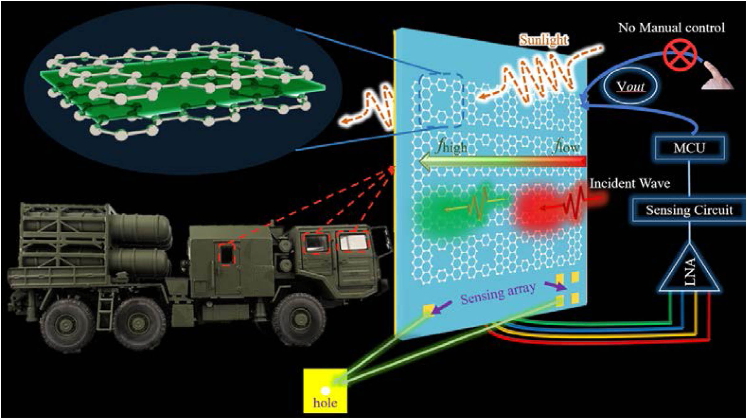
    Fig. 1. Schematic of the proposed graphene-based cognitive metasurface.
    Designed element of the graphene-based absorbing metasurface and its simulated electromagnetic response. (a) The geometrical model of unit cell that incorporates the graphene capacitor layer, the PDMS substrate, and the metal ground. (b) The top view of the unit cell. (c) The simulated absorption as a function of frequency and the sheet resistance of the graphene. (d) The simulated absorption of the proposed absorbing metasurface with the different sheet resistance of the graphene.
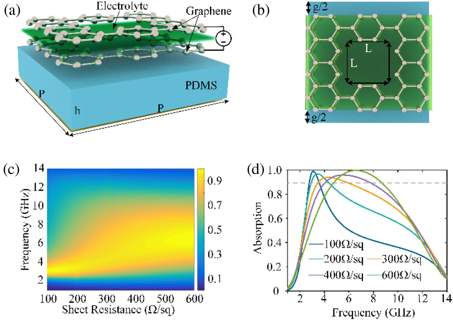
    Fig. 2. Designed element of the graphene-based absorbing metasurface and its simulated electromagnetic response. (a) The geometrical model of unit cell that incorporates the graphene capacitor layer, the PDMS substrate, and the metal ground. (b) The top view of the unit cell. (c) The simulated absorption as a function of frequency and the sheet resistance of the graphene. (d) The simulated absorption of the proposed absorbing metasurface with the different sheet resistance of the graphene.
    Electric field and current distributions and equivalent transmission-line model of the designed absorber structure. (a) The distributions of the electric field and the current density. (b) The surface current over the cross section. (c) The equivalent circuit model. (d) The analytically calculated resonant frequency. (e) The analytically calculated absorption coefficient. (f), (g) The real and imaginary parts of the calculated input impedance.
    Fig. 3. Electric field and current distributions and equivalent transmission-line model of the designed absorber structure. (a) The distributions of the electric field and the current density. (b) The surface current over the cross section. (c) The equivalent circuit model. (d) The analytically calculated resonant frequency. (e) The analytically calculated absorption coefficient. (f), (g) The real and imaginary parts of the calculated input impedance.
    Sensing mechanism of the sensing module. (a) The circuit of the sensing module. (b) The bottom view of the sensing array. (c) The top view of the sensing array. (d), (e) The measured sensing voltage versus the different frequency of the normal EM waves when the source is placed at 80 cm from the metasurface.
    Fig. 4. Sensing mechanism of the sensing module. (a) The circuit of the sensing module. (b) The bottom view of the sensing array. (c) The top view of the sensing array. (d), (e) The measured sensing voltage versus the different frequency of the normal EM waves when the source is placed at 80 cm from the metasurface.
    Photographs of the metasurface samples and experiments. (a) The photo of the experimental setup. (b) The fabricated optically transparent graphene-based absorbing metasurface. (c) The optical image of the laser-cut patterned graphene using the microscope. (d)–(f) The measured reflection coefficient at different frequencies 6.04 GHz, 5.76 GHz, and 5.56 GHz, respectively. (g)–(i) The measured absorption at different frequencies 6.04 GHz, 5.76 GHz, and 5.56 GHz, respectively.
    Fig. 5. Photographs of the metasurface samples and experiments. (a) The photo of the experimental setup. (b) The fabricated optically transparent graphene-based absorbing metasurface. (c) The optical image of the laser-cut patterned graphene using the microscope. (d)–(f) The measured reflection coefficient at different frequencies 6.04 GHz, 5.76 GHz, and 5.56 GHz, respectively. (g)–(i) The measured absorption at different frequencies 6.04 GHz, 5.76 GHz, and 5.56 GHz, respectively.
    Photographs of the metasurface sample, sensing module, and 1.8-inch LCD screen connected with the MCU. (a) The metasurface sample. (b) The 2×2 sensing array. (c) The sensing circuit. (d) The sensing voltage, frequency information, and output bias voltage displayed on the LCD screen.
    Fig. 6. Photographs of the metasurface sample, sensing module, and 1.8-inch LCD screen connected with the MCU. (a) The metasurface sample. (b) The 2×2 sensing array. (c) The sensing circuit. (d) The sensing voltage, frequency information, and output bias voltage displayed on the LCD screen.
    Mingyang Geng, Xiaolu Yang, Hao Chen, Xinzhi Bo, Mengzi Li, Zhenguo Liu, Weibing Lu. Optically transparent graphene-based cognitive metasurface for adaptive frequency manipulation[J]. Photonics Research, 2023, 11(1): 129
    Download Citation