• Photonics Research
  • Vol. 11, Issue 1, 129 (2023)
Mingyang Geng1、2, Xiaolu Yang1、2, Hao Chen1、2、4、*, Xinzhi Bo1、2, Mengzi Li1、2, Zhenguo Liu1、2、3、5、*, and Weibing Lu1、2、3、6、*
Author Affiliations
  • 1State Key Laboratory of Millimeter Waves, School of Information Science and Engineering, Southeast University, Nanjing 210096, China
  • 2Center for Flexible RF Technology, Frontiers Science Center for Mobile Information Communication and Security, Southeast University, Nanjing 210096, China
  • 3Purple Mountain Laboratories, Nanjing 211111, China
  • 4e-mail: 101300087@seu.edu.cn
  • 5e-mail: liuzhenguo@seu.edu.cn
  • 6e-mail: wblu@seu.edu.cn
  • show less
    DOI: 10.1364/PRJ.472868 Cite this Article Set citation alerts
    Mingyang Geng, Xiaolu Yang, Hao Chen, Xinzhi Bo, Mengzi Li, Zhenguo Liu, Weibing Lu. Optically transparent graphene-based cognitive metasurface for adaptive frequency manipulation[J]. Photonics Research, 2023, 11(1): 129 Copy Citation Text show less

    Abstract

    Optically transparent microwave absorbing metasurfaces have shown great potential and are needed in multiple applications environments containing optical windows owing to their ability to reduce backscattering electromagnetic (EM) signals while keeping continuous optical observation. Meanwhile, they are also required to have adaptive EM manipulation capability to cope with complex and capricious EM environments. As a general approach, distributed circuit components, including positive-intrinsic-negative diodes and varactors and sensing components, are integrated with passive absorbing metasurfaces to realize adaptive control of microwave absorption. However, these circuit elements generally require bulky electrical wires and complex control circuits to regulate the operating state, resulting in the absorbing structures being optically opaque. Hence, it is a great challenge to realize self-operating absorbers while maintaining optical transparency. Here, we report an optically transparent cognitive metasurface made of patterned graphene sandwich structures and a radio frequency detector, which can achieve adaptive frequency manipulation to match incident EM waves. As a proof-of-principle application example, we realize a closed-loop automatic absorber system prototype of the proposed graphene metasurface with self-adaptive frequency variation, without any human intervention. The approach may facilitate other adaptive metadevices in microwave regime with high-level recognition and manipulation and, more generally, promote the development of intelligent stealth technologies.

    1. INTRODUCTION

    Since World War II, microwave absorbers have been extensively reported to capture and absorb electromagnetic (EM) energy in free space. With the advent of metamaterial, a narrow-band perfect absorption metamaterial structure was proposed in 2008 [1]. Subsequently, metasurfaces, as the artificial 2D structures at surfaces or interfaces with different geometries and distributed functional arrangements, have attracted a growing attention owing to their exotic EM properties and powerful capabilities for manipulating the EM waves [27]. Different from the traditional bulk metamaterials, the features of low profile, easy fabrication, and low loss have promoted the research of metasurfaces in EM cloaks [8], vortex plates [9], retroreflectors [10], holography imaging [1114], beam shaping [15,16], anomalous deflectors [5,17], and other fascinating applications [18]. In the research mentioned above, microwave absorbing metasurface has become a hotspot because of its stealth ability for concealing objects from radar detection. Initially, the absorbing metasurfaces are passive, limited to fixed and static functionality after fabrication. With the advent and rapid development of tuning strategies, a large quantity of active absorbing metasurfaces have been designed to dynamically manipulate EM waves by integrating a variety of lumped components, such as transistors, varactors, or PIN diodes [1925]. However, the abovementioned active absorbing metasurfaces based on printed circuit board (PCB) technology and soldered by the surface mounted technology (SMT) generally require bulky power supplies, elaborate electrical wires, and complex control circuits to regulate the operating state, resulting in the optically opaque absorbing structures, which cannot be applied to various application environments containing optical windows. Actually, the optically transparent absorbers play a key role on platforms with optical windows, especially on glass windows of those ground air defense facilities and transparent windows of low detectable vehicle-mounted equipment. Recently, some advanced materials with transparent properties, including liquid crystal [26] and graphene [2734], to name a few, which provide multiple tunable or switchable functionalities, have been extensively used for being incorporated into metasurfaces to realize optically transparent reconfigurable EM response. Among these materials, graphene, as the 2D crystal, has been extensively used for electrically active metadevices owing to its unprecedented ability to control light–matter interaction over a very broad spectrum, ranging from visible to microwave frequencies [3538]. In Ref. [39], the graphene-based transparent and tunable absorbing metasurface was experimentally demonstrated. In Ref. [40], a flexible and transparent absorber with dynamical frequency modulation using graphene was observed by an experiment in the Ku band. In Ref. [41], a new class of electrically controlled active metadevices working at microwave frequencies via graphene was demonstrated. Although these multitudinous graphene-based metadevices have proved superior in steering EM waves, they are usually manually controlled by human participation.

    Self-operating devices have recently shown remarkable potential and have increased the technology’s impact. In order to achieve self-adaptability properties of fitting an external stimulus or non-stationary EM environments, the active metadevice should be further equipped with a sensing and feedback module, which can form a self-operating closed-loop system to provide desired EM responses without any human participation. In recent years, a few kinds of intelligent metasurfaces with self-adaptability properties have been reported. In Ref. [42], an intelligent microwave metasurface cloak embedded with two detectors and a deep learning network could respond rapidly to the ever-changing incident wave and surrounding background without any human intervention. In Ref. [43], the smart metasurface integrated with a power detector was proposed to adaptively modulate the reflected patterns under the different microwave incidences. In Ref. [44], an intelligent metasurface with adaptive EM functionality switching to the varying incoming wave power was demonstrated. Nevertheless, the typical approach for the above-mentioned smart metasurfaces that can dynamically control EM waves is to employ varactors or PIN diodes, which inevitably require bulky wires and complex control circuits to drive the metasurface electrically. Although more degrees of freedom in controlling EM waves, including beam shaping [45] and a dynamic polarization converter [46], can be introduced by these complex controls, there is still an inherent property of optical opaqueness, which limits their applications in multiple environments requiring continuous optical observation. Hence, it is a great challenge to realize self-operating absorbers while maintaining optical transparency. Here, we introduce and experimentally demonstrate an optically transparent graphene-based cognitive metasurface system with adaptive frequency manipulation for the first time. Such a system integrates the patterned graphene sandwich structure and EM sensing module, in which the former acts as a metasurface and is well designed to achieve a resonance frequency shift, and the latter contains a radio frequency sensing array to capture EM frequency. The two parts are connected by a micro-controller unit (MCU) managed feedback to form a closed-loop smart system, which is able to realize the self-adaptive absorption at different frequencies according to the incident EM waves without any human intervention. Numerical simulations and experimental measurements show good consistency, validating the proposed graphene-based cognitive metasurface.

    2. DESIGN AND METHODS

    A. Principle of the Cognitive Metasurface

    We propose an optically transparent graphene-based cognitive metasurface system for adaptive microwave camouflage, which evolves from the graphene-based absorbing metasurface, with self-recognitions and manipulations on the frequency of EM waves. Figure 1 provides a schematic of the presented metasurface, which is composed of the sensing module and frequency-tunable absorbing structure. Under the illumination of a plane wave, the sensing array is able to recognize the incident frequency information and transmit the data to the MCU. After collecting the data, the MCU will determine and provide the voltage on the graphene sandwich structure to generate the desired EM absorption. According to the frequency information from the sensing data, the metasurface can realize resonance frequency manipulation based on the pre-designed procedure. The frequency manipulation of the absorbing structure is driven by the graphene capacitor layer under voltage control. The graphene capacitor is the sandwich structure that consists of two patterned graphene films separated by the electrolyte layer, as shown in the illustration in Fig. 1. When the electrostatic field bias is applied to the graphene capacitor, the electrolyte layer polarizes and ionic double layers form on the graphene-electrolyte interface with opposite polarizations, leading to tunable high-mobility free carriers on the graphene sheets that can respond to microwaves [37]. As a result, the Fermi energy of the graphene will be tuned, and the sheet resistance of the graphene changes correspondingly.

    Schematic of the proposed graphene-based cognitive metasurface.

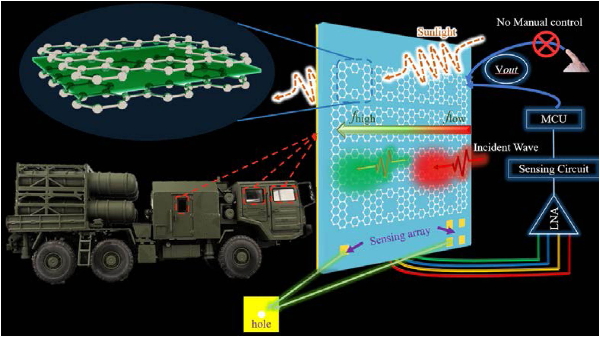
    Figure 1.Schematic of the proposed graphene-based cognitive metasurface.

    B. Design of the Graphene-Based Metasurface with Frequency Manipulation

    To achieve a frequency tunable absorbing metasurface, the elaborately patterned graphene is applied in the element design, as shown in Figs. 2(a) and 2(b). The geometrical structure of the proposed absorbing metasurface is mainly composed of three components: the patterned graphene sandwich structure, the polydimethylsiloxane (PDMS) substrate layer, and a metallic wire mesh ground. The patterned graphene sandwich structure is composed of two of the same patterned graphene sheets transferred on the flexible and microwave-transparent polyethylene terephthalate (PET) substrate and with an electrolyte sandwiched between them. The metal wire mesh ground here is to block and trap the transmitted EM waves. The period P is 7.5 mm, and the height h is 6 mm, and the dielectric constant of the PDMS is 2.8 with a tangential loss of 0.02. The graphene sheets are designed as the grid patterns, which are utilized to adjust the resonant state. When introducing the external bias voltage on the patterned graphene capacitor, the sheet resistance of graphene will be changed, which influences the input impedance of the absorbing structure. As a consequence, the tunable radar absorber can be achieved with the dynamically tunable frequency. Figure 2(b) shows the specific pattern of the graphene, in which the gap of g between the adjacent units is 0.2 mm and the grid length is L=1  mm. The numerical simulation of the absorbing structure is accomplished by the commercial software CST Microwave Studio. The periodic boundary condition is set to its four lateral sides for modeling the infinite array, and the Floquet ports are chosen along the z-direction. The graphene can be approximately considered as a resistive sheet without dispersion at the microwave frequencies, which is generally regarded as a variable ohmic sheet in the numerical analysis [47]. Figure 2(c) shows the simulated absorption as a function of the frequency and the sheet resistance of the graphene. It is obvious that the resonance frequency can be dynamically tuned over a wide frequency band. When the graphene resistance varies from 100 to 600 Ω/sq, the corresponding resonant frequency increases from 3.09 to 6.59 GHz. Simultaneously, the absorption coefficient corresponding to the resonant frequency remains above 0.9, thus realizing a frequency tunable perfect absorption. Figure 2(d) reveals the curves of the absorption coefficient when the graphene resistance is chosen as 100, 200, 300, 400, and 600 Ω/sq, respectively. It is seen that the resonance frequency is red shifted, monotonically decreasing as the graphene resistance decreases, which is consistent with results in Fig. 2(c), as well as the high absorption coefficient at different resonant frequency.

    Designed element of the graphene-based absorbing metasurface and its simulated electromagnetic response. (a) The geometrical model of unit cell that incorporates the graphene capacitor layer, the PDMS substrate, and the metal ground. (b) The top view of the unit cell. (c) The simulated absorption as a function of frequency and the sheet resistance of the graphene. (d) The simulated absorption of the proposed absorbing metasurface with the different sheet resistance of the graphene.

    Figure 2.Designed element of the graphene-based absorbing metasurface and its simulated electromagnetic response. (a) The geometrical model of unit cell that incorporates the graphene capacitor layer, the PDMS substrate, and the metal ground. (b) The top view of the unit cell. (c) The simulated absorption as a function of frequency and the sheet resistance of the graphene. (d) The simulated absorption of the proposed absorbing metasurface with the different sheet resistance of the graphene.

    To investigate the detailed absorption mechanism of the proposed absorbing metasurface, the distributions of the electrical field and the current density corresponding to the absorption peak at 6.59 GHz are simulated, as illustrated in Fig. 3(a). Figure 3(a) shows that strong electric field energy is localized in the gaps of adjacent graphene patterns, which induces electric resonance. Meanwhile, the arrows representing the energy flow accumulate mainly in the edges of the graphene layer, which is consistent with the phenomenon on electrical field distribution. Figure 3(b) reveals the surface current distributions on the graphene and the ground layer at 6.59 GHz, in which the surface currents flow in an opposite direction, thus forming the magnetic resonance. Therefore, the perfect absorption at 6.59 GHz results from both electric and magnetic resonances, and most of the incident EM energy is dissipated because of the high ohmic loss of the graphene layer. Additionally, an equivalent transmission-line (TL) model with the specific lumped circuit elements is presented to quantificationally analyze the EM resonant characteristic of the designed absorbing structure, which could give us more intuitive insight into the operation principle, as displayed in Fig. 3(c). The patterned graphene layer in the sandwich structure is modeled as a series of connections of a variable resistor (Rg), an inductor (Lg), and a capacitor (Cg), in which the equivalent resistance Rg is voltage-dependent, and the values of Lg and Cg are obtained by parameter fitting in the commercial Advanced Design System (ADS). The optimized values of Lg and Cg are 0.001 nH and 0.174 pF, respectively. Reflection, due to the electrolyte, is negligible because the ions of the electrolyte have very low mobility. Therefore, they cannot respond to the electric field of microwaves [37]. The cascaded transmission lines with the characteristic impedances Z1, Z2, and Z3 are utilized to model different kinds of substrates, including PET, diaphragm paper, and PDMS, respectively. In addition, the ground layer is represented by a short TL. Hence, the equivalent impedance of the patterned graphene sandwich structure can be analytically expressed as Zg=(Rg+jωLg+1jωCg)(Rg+jωLg+1jωCg),in which Rg=RoP2(Pg)2L2.

    Electric field and current distributions and equivalent transmission-line model of the designed absorber structure. (a) The distributions of the electric field and the current density. (b) The surface current over the cross section. (c) The equivalent circuit model. (d) The analytically calculated resonant frequency. (e) The analytically calculated absorption coefficient. (f), (g) The real and imaginary parts of the calculated input impedance.

    Figure 3.Electric field and current distributions and equivalent transmission-line model of the designed absorber structure. (a) The distributions of the electric field and the current density. (b) The surface current over the cross section. (c) The equivalent circuit model. (d) The analytically calculated resonant frequency. (e) The analytically calculated absorption coefficient. (f), (g) The real and imaginary parts of the calculated input impedance.

    The total input impedance of Zin is a cascade of Zg and other TLs representing the substrate, which can be calculated based upon the transmission line theory. When the normally incident EM wave illuminates the absorbing metasurface, the absorption can be deduced as A=1|(Zinη0)/(Zin+η0)|2.

    Figure 3(e) depicts the calculated absorption of the proposed absorbing structure under different sheet resistances of the graphene layer, in which the solid and dotted lines represent the simulation and calculation results, respectively. It is seen that the calculated results show a high consistency with the simulated ones. In the meantime, the trends of peak absorptivity and resonance frequency between simulated and analytical results are displayed in Fig. 3(d). Here, absorption peaks are seen to coincide within an error range of 1.2%, and the calculated resonance frequency accords closely with simulation. Apparently, all these results verify the accuracy of the presented TL model. The analytical results, including the real and the imaginary components of the equivalent input impedance Zin, are evaluated, as exhibited in Figs. 3(f) and 3(g). For the normally incident plane wave, perfect absorption occurs while Zin matches the following conditions {Re(Zin)=ηo=120πIm(Zin)=0.

    It can be seen in Fig. 3(g) that the operation frequency corresponding to the point of Im(Zin)=0 shifts from 6.72 to 3.09 GHz as graphene resistance decreases. Simultaneously, the values of the real part of Zin in Fig. 3(f) at the above operation frequency are nearly close to 120π  Ω, thus leading to a nearly perfect absorption as well as dynamical frequency manipulation. In conclusion, the results enumerated through the TL model in Fig. 3 show a good agreement with those in Fig. 2, which demonstrates that the principle of dynamical frequency manipulation by tuning the surface resistance of a graphene metasurface is scientifically sound.

    C. Design of the Sensing Module

    To clearly expound on the sensing mechanism of the sensing module, the exhaustive sensing circuit and sensing array are explicitly provided in Fig. 4. The radio frequency power detector, LTC5530, is chosen to convert EM energy into a voltage signal, around which the lumped components are cascaded to obtain a direct current (DC) signal. Figures 4(b) and 4(c) show the bottom and top views of the sensing array, respectively, in which two metal-coated via holes are utilized to capture incident EM energy. The sensing array is illuminated by the horn connecting with the signal source, as shown in Fig. 4(d). The power level of the captured EM energy from via holes in the sensing array is very low, so the received EM energy is firstly sent to a cascaded low noise amplifier (LNA) and a limiter, which will increase and set the appropriate power level going into the RFin through the welded Sub-Miniature-A (SMA). In the measurement, the DC voltage can be acquired by a voltmeter connecting to Vout of the sensing circuit. The tested results between the final output voltage Vout and the input EM frequency are given in Fig. 4(e). The linear relationship between the output voltage and frequency is obtained, and there is no overlap of the DC voltage within a broad bandwidth from 5.0 to 6.0 GHz. Subsequently, the output voltage can be recognized by MCU, which means the input frequency information has been perceived according to the relationship in Fig. 4(e). After collecting the frequency information, the MCU will determine and provide the feedback voltages on the graphene capacitor of the absorbing structure to generate the desired absorption corresponding to incident EM waves. Therefore, the experimental results verified that the designed sensing module can detect the frequency band from 5 to 6.2 GHz, which will offer an authoritative input for the smart frequency manipulation for adaptive microwave camouflage using the above graphene-based absorbing metasurface.

    Sensing mechanism of the sensing module. (a) The circuit of the sensing module. (b) The bottom view of the sensing array. (c) The top view of the sensing array. (d), (e) The measured sensing voltage versus the different frequency of the normal EM waves when the source is placed at 80 cm from the metasurface.

    Figure 4.Sensing mechanism of the sensing module. (a) The circuit of the sensing module. (b) The bottom view of the sensing array. (c) The top view of the sensing array. (d), (e) The measured sensing voltage versus the different frequency of the normal EM waves when the source is placed at 80 cm from the metasurface.

    3. EXPERIMENTAL MEASUREMENT AND DISCUSSION

    To experimentally demonstrate the proposed concepts and designs, a closed-loop automatic absorbing metasurface prototype with a frequency sensing and feedback system was fabricated, as shown in Fig. 5(a). The sensing and feedback system consists of the cascaded LNA and limiter to provide a steady power level into the sensing circuit, and the MCU will collect frequency information and feed appropriate voltages to the absorbing structure, as exhibited in Appendix A. Benefiting from the transparency of the graphene, the PDMS, and the wire mesh ground, the final absorbing structure in Fig. 5(b) displays the optically transparent characteristic. The size of the absorber sample is 150  mm×150  mm, and the optical image of the laser-cut patterned graphene coated on PET is presented in Fig. 5(c). The experiments are carried out in a semi-enclosed microwave anechoic chamber, in which two linearly polarized horn antennas, working from 2 to 18 GHz, are employed as the transmitting and receiving antennas. The distance between the sample and transmitting horn antenna is 90 cm. In the measurement, the transmitting horn provides the excitation signal at a fixed frequency. The MCU (STM32F407) is utilized to collect the incident frequency information from the sensing circuit and generate opportune bias voltages applied on the absorbing metasurface. For the sake of observation, the related information is displayed on a 1.8-inch LCD screen, as illustrated in Appendix A. In addition, in order to better exhibit the absorption corresponding to different incident frequencies, we measured the frequency band response by measuring the reflection parameter through the receiving antenna connected to a vector network analyzer. The wire mesh with the same size of the absorber sample is firstly measured to calibrate the reflection spectrum. The response time of the whole process, from sensing to feedback frequency manipulation, depends on the time for the graphene sandwich structure to achieve the steady state while applying bias voltages, which is nearly 330 ms [37]. The time from sensing to feedback voltage is practically in real-time within 1 ms, which is negligible compared to the above time. Figures 5(g)–5(i) show the measured absorption according to the reflection coefficient when the incident frequency is chosen as 5.5 GHz, 5.7 GHz, and 6.0 GHz, respectively, in which markers at 5.56 GHz, 5.76 GHz, and 6.04 GHz represent the measured resonance frequency. Although there are some deviations between incident frequency and those measured, the experimental results demonstrate that the smart frequency manipulation function is realized, thus achieving the self-adaptive absorption at different frequencies according to the incident EM waves without any human intervention.

    Photographs of the metasurface samples and experiments. (a) The photo of the experimental setup. (b) The fabricated optically transparent graphene-based absorbing metasurface. (c) The optical image of the laser-cut patterned graphene using the microscope. (d)–(f) The measured reflection coefficient at different frequencies 6.04 GHz, 5.76 GHz, and 5.56 GHz, respectively. (g)–(i) The measured absorption at different frequencies 6.04 GHz, 5.76 GHz, and 5.56 GHz, respectively.

    Figure 5.Photographs of the metasurface samples and experiments. (a) The photo of the experimental setup. (b) The fabricated optically transparent graphene-based absorbing metasurface. (c) The optical image of the laser-cut patterned graphene using the microscope. (d)–(f) The measured reflection coefficient at different frequencies 6.04 GHz, 5.76 GHz, and 5.56 GHz, respectively. (g)–(i) The measured absorption at different frequencies 6.04 GHz, 5.76 GHz, and 5.56 GHz, respectively.

    Notwithstanding, there are still two aspects to be considered to improve this research. On the one hand, the proposed cognitive metasurface is not integrated enough. This is mainly because it is challenging and not easy to weld semiconductor elements, including the capacitor and the resistor, and achieve metal-coated via holes on flexible dielectric substrates such as PDMS. Hence, the sensing module composed of the sensing array and the sensing circuit in this research is fabricated using printed circuit board technology. As a result, the proposed graphene-based cognitive metasurface system is divided into two parts: one is the optically transparent graphene metasurface, and the other is the sensing and feedback module. In future research, the hybrid design strategies and some advanced processing technologies will be considered for finishing the integration of the above two parts. In addition, the optical characteristic is helpful for solar energy collection. Therefore, making the flexible solar panel cooperate with the transparent graphene-based cognitive metasurface to realize a self-powered closed-loop automatic absorber system will be studied further. On the other hand, the meta-atom of the absorbing metasurface is designed for single polarization waves. Therefore, the proposed metasurface can sense and control the frequency manipulation of single polarization EM waves. The design of dual polarization and polarization-insensitive metasurfaces will be researched in further studies.

    4. CONCLUSION

    We have proposed an optically transparent graphene-based cognitive metasurface, which can realize the smart frequency manipulation for adaptive microwave camouflage. By integrating the EM frequency sensing module and the MCU-managed feedback system, the graphene-based absorbing metasurface can automatically change its absorption property to match the incoming EM waves according to the customized frequency dependent functions correspondingly. Meanwhile, the experimental results demonstrate a closed-loop automatic absorber system with smart frequency manipulation for the first time. We believe that this work will further encourage research on graphene-based cognitive metasurfaces with more complicated and more high-level EM controls by incorporating coding and programmable graphene [30,48], and more generally, promote the development of intelligent stealth and camouflage in the microwave regime.

    5. EXPERIMENTAL SECTION

    A. Fabrication of the Patterned Graphene Metasurface

    The graphene film was grown on copper foil using the chemical vapor deposition method and then transferred onto a 0.125-mm-thick PET film. The pattern on the graphene film was etched by a UV laser. Then, the large-area graphene-coated PET substrate was finished and prepared to serve as the electrode of the graphene sandwich structure. Finally, a piece of diaphragm paper (thickness 50 μm) from NKK-TF40 infiltrated with 20 μL of ionic liquid was sandwiched between two graphene-coated PET electrodes. The disturbance to reflectance of the proposed absorbing metasurface from the electrode layer can be negligible owing to its small thickness, far less than our operation wavelength of 50 mm (6 GHz). Thus, the fabrication of the patterned graphene metasurface was achieved.

    B. Measurement

    The reflection characteristic of the sample was measured in an in-house semi-enclosed microwave anechoic chamber to minimize the noise wave in the environment. Two linearly polarized wideband horn antennas were respectively set as receiver and transmitter. The transmitting horn generated a quasi-plane wave to illuminate the sample, and the reflected wave energy was captured by the receiving horn. The reflection spectrum of the sample was obtained by measuring the transmission between two horn antennas. In the reflection measurement, the setup was normalized by the wire mesh ground with the same size of the absorber sample as a perfect reflecting mirror.

    APPENDIX A: THE DETAILS OF THE FABRICATED SAMPLE

    More details about the fabricated closed-loop automatic absorbing metasurface prototype with the frequency sensing and feedback system are shown in Fig. 6. The dimension of the sensing array is 40  mm×40  mm. Additionally, the sensing circuit is presented in Fig. 6(c). For the sake of observation, the incident frequency from the sensing circuit and the bias voltages applied on the absorbing metasurface are displayed on a 1.8-inch LCD screen, as recorded in Fig. 6(d).

    Photographs of the metasurface sample, sensing module, and 1.8-inch LCD screen connected with the MCU. (a) The metasurface sample. (b) The 2×2 sensing array. (c) The sensing circuit. (d) The sensing voltage, frequency information, and output bias voltage displayed on the LCD screen.

    Figure 6.Photographs of the metasurface sample, sensing module, and 1.8-inch LCD screen connected with the MCU. (a) The metasurface sample. (b) The 2×2 sensing array. (c) The sensing circuit. (d) The sensing voltage, frequency information, and output bias voltage displayed on the LCD screen.

    References

    [1] N. I. Landy, S. Sajuyigbe, J. J. Mock, D. R. Smith, W. J. Padilla. Perfect metamaterial absorber. Phys. Rev. Lett., 100, 207402(2008).

    [2] N. Yu, P. Genevet, M. A. Kats, F. Aieta, J.-P. Tetienne, F. Capasso, Z. Gaburro. Light propagation with phase discontinuities: generalized laws of reflection and refraction. Science, 334, 333-337(2011).

    [3] T. J. Cui, M. Q. Qi, X. Wan, J. Zhao, Q. Cheng. Coding metamaterials, digital metamaterials and programmable metamaterials. Light Sci. Appl., 3, e218(2014).

    [4] L. Zhang, S. Mei, K. Huang, C.-W. Qiu. Advances in full control of electromagnetic waves with metasurfaces. Adv. Opt. Mater., 4, 818-833(2016).

    [5] L. Zhang, R. Y. Wu, G. D. Bai, H. T. Wu, Q. Ma, X. Q. Chen, T. J. Cui. Transmission-reflection-integrated multifunctional coding metasurface for full-space controls of electromagnetic waves. Adv. Funct. Mater., 28, 1802205(2018).

    [6] S. Chen, Z. Li, W. Liu, H. Cheng, J. Tian. From single-dimensional to multidimensional manipulation of optical waves with metasurfaces. Adv. Mater., 31, 1802458(2019).

    [7] J. W. Wu, Z. X. Wang, Z. Q. Fang, J. C. Liang, X. Fu, J. F. Liu, H. T. Wu, D. Bao, L. Miao, X. Y. Zhou, Q. Cheng, T. J. Cui. Full-State synthesis of electromagnetic fields using high efficiency phase-only metasurfaces. Adv. Funct. Mater., 30, 2004144(2020).

    [8] B. Orazbayev, N. Mohammadi Estakhri, A. Alù, M. Beruete. Experimental demonstration of metasurface-based ultrathin carpet cloaks for millimeter waves. Adv. Opt. Mater., 5, 1600606(2017).

    [9] M. Q. Mehmood, S. Mei, S. Hussain, K. Huang, S. Y. Siew, L. Zhang, T. Zhang, X. Ling, H. Liu, J. Teng, A. Danner, S. Zhang, C.-W. Qiu. Visible-frequency metasurface for structuring and spatially multiplexing optical vortices. Adv. Mater., 28, 2533-2539(2016).

    [10] A. Arbabi, E. Arbabi, Y. Horie, S. M. Kamali, A. Faraon. Planar metasurface retroreflector. Nat. Photonics, 11, 415-420(2017).

    [11] G. Zheng, H. Mühlenbernd, M. Kenney, G. Li, T. Zentgraf, S. Zhang. Metasurface holograms reaching 80% efficiency. Nat. Nanotechnol., 10, 308-312(2015).

    [12] J. S. Park, J. Lee, E. S. Jung, M.-H. Kim, I. B. Kim, H. Son, S. Kim, S. Kim, Y. M. Park, I. Mook-Jung, S. J. Yu, J. H. Lee. Brain somatic mutations observed in Alzheimer’s disease associated with aging and dysregulation of tau phosphorylation. Nat. Commun., 10, 3090(2019).

    [13] W. T. Chen, A. Y. Zhu, J. Sisler, Y.-W. Huang, K. M. A. Yousef, E. Lee, C.-W. Qiu, F. Capasso. Broadband achromatic metasurface-refractive optics. Nano Lett., 18, 7801-7808(2018).

    [14] G.-Y. Lee, J.-Y. Hong, S. Hwang, S. Moon, H. Kang, S. Jeon, H. Kim, J.-H. Jeong, B. Lee. Metasurface eyepiece for augmented reality. Nat. Commun., 9, 1(2018).

    [15] H.-H. Hsiao, C. H. Chu, D. P. Tsai. Fundamentals and applications of metasurfaces. Small Methods, 1, 1600064(2017).

    [16] X. Xie, X. Li, M. Pu, X. Ma, K. Liu, Y. Guo, X. Luo. Plasmonic metasurfaces for simultaneous thermal infrared invisibility and holographic illusion. Adv. Funct. Mater., 28, 1706673(2018).

    [17] K. Zhang, Y. Yuan, X. Ding, B. Ratni, S. Nawaz Burokur, Q. Wu. High-efficiency metalenses with switchable functionalities in microwave region. ACS Appl. Mater. Interf., 11, 28423-28430(2019).

    [18] S. Sun, Q. He, J. Hao, S. Xiao, L. Zhou. Electromagnetic metasurfaces: physics and applications. Adv. Opt. Photon., 11, 380-479(2019).

    [19] J. Y. Lau, S. V. Hum. A wideband reconfigurable transmitarray element. IEEE Trans. Antenn. Propag., 60, 1303-1311(2011).

    [20] C. Huang, W. Pan, X. Ma, B. Zhao, J. Cui, X. Luo. Using reconfigurable transmitarray to achieve beam-steering and polarization manipulation applications. IEEE Trans. Antenn. Propag., 63, 4801-4810(2015).

    [21] C. Huang, C. Zhang, J. Yang, B. Sun, B. Zhao, X. Luo. Reconfigurable metasurface for multifunctional control of electromagnetic waves. Adv. Opt. Mater., 5, 1700485(2017).

    [22] X. Gao, W. L. Yang, H. F. Ma, Q. Cheng, X. H. Yu, T. J. Cui. A reconfigurable broadband polarization converter based on an active metasurface. IEEE Trans. Antennas Propag., 66, 6086-6095(2018).

    [23] R. Phon, S. Ghosh, S. Lim. Novel multifunctional reconfigurable active frequency selective surface. IEEE Trans. Antennas Propag., 67, 1709-1718(2019).

    [24] G. Y. Liu, L. Li, J. Q. Han, H. X. Liu, X. H. Gao, Y. Shi, T. J. Cui. Frequency-domain and spatial-domain reconfigurable metasurface. ACS Appl. Mater. Interf., 12, 23554-23564(2020).

    [25] L. W. Wu, H. F. Ma, R. Wu, Q. Xiao, Y. Gou, M. Wang, Z. X. Wang, L. Bao, H. L. Wang, Y. M. Qing, T. J. Cui. Transmission-reflection controls and polarization controls of electromagnetic holograms by a reconfigurable anisotropic digital coding metasurface. Adv. Opt. Mater., 8, 2001065(2020).

    [26] G. Perez-Palmino, P. Baine, M. Bain, J. A. Encinar, R. Cahill, M. Barba, G. Toso. Design and experimental validation of liquid crystal-based reconfigurable reflectarray elements with improved bandwidth in F-band. IEEE Trans. Antennas Propag., 61, 1704-1713(2013).

    [27] H. Chen, W.-B. Lu, Z.-G. Liu, Z. H. Jiang. Flexible rasorber based on graphene with energy manipulation function. IEEE Trans. Antennas Propag., 68, 351-359(2020).

    [28] M.-Y. Geng, Z.-G. Liu, W.-J. Wu, H. Chen, B. Wu, W.-B. Lu. A dynamically tunable microwave absorber based on graphene. IEEE Trans. Antennas Propag., 68, 4706-4713(2020).

    [29] J. Zhang, X. Wei, I. D. Rukhlenko, H.-T. Chen, W. Zhu. Electrically tunable metasurface with independent frequency and amplitude modulations. ACS Photon., 7, 265-271(2020).

    [30] J. Zhang, H. Zhang, W. Yang, K. Chen, X. Wei, Y. Feng, R. Jin, W. Zhu. Dynamic scattering steering with graphene-based coding metamirror. Adv. Opt. Mater., 8, 2000683(2020).

    [31] C. Huang, J. Song, C. Ji, J. Yang, X. Luo. Simultaneous control of absorbing frequency and amplitude using graphene capacitor and active frequency-selective surface. IEEE Trans. Antennas Propag., 69, 1793-1798(2021).

    [32] C. Huang, J. Liao, C. Ji, J. Peng, L. Yuan, X. Luo. Graphene-integrated reconfigurable metasurface for independent manipulation of reflection magnitude and phase. Adv. Opt. Mater., 9, 2001950(2021).

    [33] C. Huang, C. Ji, B. Zhao, J. Peng, L. Yuan, X. Luo. Multifunctional and tunable radar absorber based on graphene-integrated active metasurface. Adv. Mater. Technol., 6, 2001050(2021).

    [34] C. Huang, J. Yang, C. Ji, L. Yuan, X. Luo. Graphene-driven metadevice for active microwave camouflage with high-efficiency transmission window. Small Methods, 5, 2000918(2021).

    [35] N. Rouhi, S. Capdevila, D. Jain, K. Zand, Y. Y. Wang, E. Brown, L. Jofre, P. Burke. Terahertz graphene optics. Nano Res., 5, 667-678(2012).

    [36] B. Wu, H. M. Tuncer, M. Naeem, B. Yang, M. T. Cole, W. I. Milne, Y. Hao. Experimental demonstration of a transparent graphene millimetre wave absorber with 28% fractional bandwidth at 140 GHz. Sci. Rep., 4, 4130(2014).

    [37] O. Balci, E. O. Polat, N. Kakenov, C. Kocabas. Graphene-enabled electrically switchable radar-absorbing surfaces. Nat. Commun., 6, 6628(2015).

    [38] S. Kim, M. S. Jang, V. W. Brar, K. W. Mauser, L. Kim, H. A. Atwater. Electronically tunable perfect absorption in graphene. Nano Lett., 18, 971-979(2018).

    [39] J. Zhang, Z. Li, L. Shao, W. Zhu. Dynamical absorption manipulation in a graphene-based optically transparent and flexible metasurface. Carbon, 176, 374-382(2021).

    [40] M. Y. Geng, H. Chen, Z. G. Liu, W. B. Lu, X. L. Yang, X. Z. Bao. Transparent and flexible absorber with dynamically frequency modulation using graphene. IEEE 4th International Conference on Electronic Information and Communication Technology (ICEICT), 840-842(2021).

    [41] O. Balci, N. Kakenov, E. Karademir, S. Balci, S. Cakmakyapan, E. O. Polat, H. Caglayan, E. Özbay, C. Kocabas. Electrically switchable metadevices via graphene. Sci. Adv., 4, eaao1749(2018).

    [42] C. Qian, B. Zheng, Y. Shen, L. Jing, E. Li, L. Shen, H. Chen. Deep-learning-enabled self-adaptive microwave cloak without human intervention. Nat. Photonics, 14, 383-390(2020).

    [43] Q. Ma, Q. R. Hong, X. X. Gao, H. B. Jing, C. Liu, G. D. Bai, Q. Cheng, T. J. Cui. Smart sensing metasurface with self-defined functions in dual polarizations. Nanophotonics, 9, 3271-3278(2020).

    [44] Y. She, C. Ji, C. Huang, Z. Zhang, J. Liao, J. Wang, X. Luo. Intelligent reconfigurable metasurface for self-adaptively electromagnetic functionality switching. Photon. Res., 10, 769-776(2022).

    [45] B. Ratni, A. de Lustrac, G.-P. Piau, S. N. Burokur. Reconfigurable meta-mirror for wavefronts control: applications to microwave antennas. Opt. Express, 26, 2613-2624(2018).

    [46] Q. Hu, K. Chen, N. Zhang, J. Zhao, T. Jiang, J. Zhao, Y. Feng. Arbitrary and dynamic poincaré sphere polarization converter with a time-varying metasurface. Adv. Opt. Mater., 10, 2101915(2022).

    [47] M. Geng, Z. Liu, H. Chen, X. Bao, X. Yang, W. Lu. Flexible and dual-tunable radar absorber enabled by graphene. Adv. Mater. Technol., 7, 2200028(2022).

    [48] H. Chen, W.-B. Lu, Z.-G. Liu, M.-Y. Geng. Microwave programmable graphene metasurface. ACS Photon., 7, 1425-1435(2020).

    Mingyang Geng, Xiaolu Yang, Hao Chen, Xinzhi Bo, Mengzi Li, Zhenguo Liu, Weibing Lu. Optically transparent graphene-based cognitive metasurface for adaptive frequency manipulation[J]. Photonics Research, 2023, 11(1): 129
    Download Citation