• Journal of Infrared and Millimeter Waves
  • Vol. 41, Issue 2, 464 (2022)
Zhen-Bing DAI1、2, Guo-Yu LUO2, Yan HE2, Chong WANG3、4, Hu-Gen YAN3、4, and Zhi-Qiang LI2、*
Author Affiliations
  • 1Department of Physics,Sichuan Normal University,Chengdu 610066
  • 2College of Physics,Sichuan University,Chengdu 610065,China
  • 3State Key Laboratory of Applied Surface Physics,Fudan University,Shanghai 200438,China
  • 4Department of Physics,Fudan University,Shanghai 200438,China
  • show less
    DOI: 10.11972/j.issn.1001-9014.2022.02.013 Cite this Article
    Zhen-Bing DAI, Guo-Yu LUO, Yan HE, Chong WANG, Hu-Gen YAN, Zhi-Qiang LI. Near-field imaging of WTe2[J]. Journal of Infrared and Millimeter Waves, 2022, 41(2): 464 Copy Citation Text show less
    Schematic of the set-up of s-SNOM
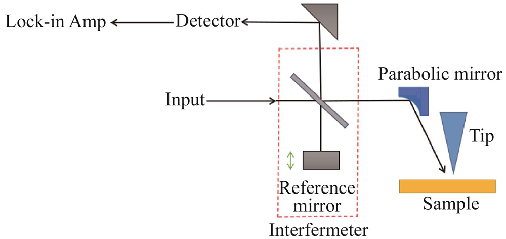
    Fig. 1. Schematic of the set-up of s-SNOM
    Near-filed signal of WTe2 thin film of different sample thickness at different incident light frequency(a)70 nm,910cm-1;(b)56 nm,1 550 cm-1;(c)52 nm,910 cm-1;(d)26 nm,1 550 cm-1
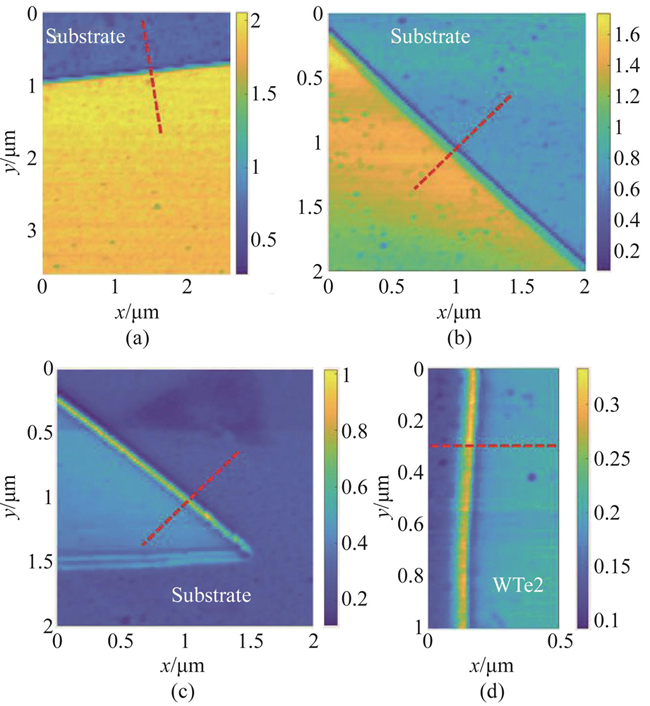
    Fig. 2. Near-filed signal of WTe2 thin film of different sample thickness at different incident light frequency(a)70 nm,910cm-1;(b)56 nm,1 550 cm-1;(c)52 nm,910 cm-1;(d)26 nm,1 550 cm-1
    (a)-(d)correspond to the topography of WTe2(black curve)and its O3A profile(red curve)along red dash line in figure 2,respectively
    Fig. 3. (a)-(d)correspond to the topography of WTe2(black curve)and its O3A profile(red curve)along red dash line in figure 2,respectively
    The IR reflectance and optical conductance of WTe2 fitting by Drude-Lorentz model(a)IR reflectance fitting of WTe2 at 295 K,(b)IR conductance fitting of WTe2 at same temperature
    Fig. 4. The IR reflectance and optical conductance of WTe2 fitting by Drude-Lorentz model(a)IR reflectance fitting of WTe2 at 295 K,(b)IR conductance fitting of WTe2 at same temperature
    The real and imaginary part of dielectric function fitting of WTe2
    Fig. 5. The real and imaginary part of dielectric function fitting of WTe2
    Illumination of tip-sample scattering in finite-dipole model
    Fig. 6. Illumination of tip-sample scattering in finite-dipole model
    The ratio of sample/substrate near field signal with different sample thickness at different incident frequency. Note:The hollow data point is the result of signal enhancement at the edge of the sample
    Fig. 7. The ratio of sample/substrate near field signal with different sample thickness at different incident frequency. Note:The hollow data point is the result of signal enhancement at the edge of the sample
    Zhen-Bing DAI, Guo-Yu LUO, Yan HE, Chong WANG, Hu-Gen YAN, Zhi-Qiang LI. Near-field imaging of WTe2[J]. Journal of Infrared and Millimeter Waves, 2022, 41(2): 464
    Download Citation