• Photonics Research
  • Vol. 11, Issue 2, 189 (2023)
Rongxiang Guo1、2, Shujiao Zhang1、2, Haoran Gao1、2, Ganapathy Senthil Murugan3, Tiegen Liu1、2, and Zhenzhou Cheng1、2、4、5、*
Author Affiliations
  • 1School of Precision Instruments and Optoelectronics Engineering, Tianjin University, Tianjin 300072, China
  • 2Key Laboratory of Optoelectronics Information Technology, Ministry of Education, Tianjin 300072, China
  • 3Optoelectronics Research Centre, University of Southampton, Southampton SO17 1BJ, UK
  • 4Georgia Tech-Shenzhen Institute, Tianjin University, Shenzhen 518055, China
  • 5Department of Chemistry, The University of Tokyo, Tokyo 113-0033, Japan
  • show less
    DOI: 10.1364/PRJ.474199 Cite this Article Set citation alerts
    Rongxiang Guo, Shujiao Zhang, Haoran Gao, Ganapathy Senthil Murugan, Tiegen Liu, Zhenzhou Cheng. Blazed subwavelength grating coupler[J]. Photonics Research, 2023, 11(2): 189 Copy Citation Text show less
    Schematic of the BSWG coupler in (a) 3D view, (b) cross-section view, and (c) top view. BSWGs in the y direction can be treated as a homogenous EM when Λy is smaller than the light wavelength.
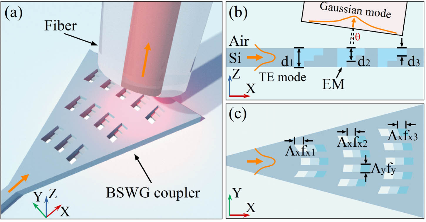
    Fig. 1. Schematic of the BSWG coupler in (a) 3D view, (b) cross-section view, and (c) top view. BSWGs in the y direction can be treated as a homogenous EM when Λy is smaller than the light wavelength.
    Simulation results of SWG couplers. (a) Directionality of uniform BSWG couplers with different parameter combinations of fx and fy. Here, fxa, fxb, and fxc are [0.20, 0.50, 0.15], [0.30, 0.40, 0.15], and [0.40, 0.30, 0.15], respectively. (b) Coupling efficiencies of the single-step-etched SWG coupler, uniform BSWG coupler, and apodized BSWG coupler as a function of wavelength. (c) Grating diffracted electric-field distributions of the single-step-etched SWG coupler (i), uniform BSWG (ii), and apodized BSWG coupler (iii).
    Fig. 2. Simulation results of SWG couplers. (a) Directionality of uniform BSWG couplers with different parameter combinations of fx and fy. Here, fxa, fxb, and fxc are [0.20, 0.50, 0.15], [0.30, 0.40, 0.15], and [0.40, 0.30, 0.15], respectively. (b) Coupling efficiencies of the single-step-etched SWG coupler, uniform BSWG coupler, and apodized BSWG coupler as a function of wavelength. (c) Grating diffracted electric-field distributions of the single-step-etched SWG coupler (i), uniform BSWG (ii), and apodized BSWG coupler (iii).
    SEM images of uniform and apodized BSWG couplers. (a) Top view of the uniform grating coupler. (b) Top view of the apodized BSWG coupler. (c) Zoom-in image of one period of the uniform BSWG coupler. (d) Zoom-in image of one period of the apodized BSWG coupler.
    Fig. 3. SEM images of uniform and apodized BSWG couplers. (a) Top view of the uniform grating coupler. (b) Top view of the apodized BSWG coupler. (c) Zoom-in image of one period of the uniform BSWG coupler. (d) Zoom-in image of one period of the apodized BSWG coupler.
    Experimental results and 3D-FDTD simulations of uniform and apodized BSWG couplers. (a) Coupling spectrum of the uniform BSWG coupler with fx of [0.40, 0.30, 0.15] and fy of 0.5. (b) Coupling spectrum of the apodized BSWG coupler. The maximum coupling efficiency of −4.53 dB with the 3-dB bandwidth of ∼107 nm was measured at the center wavelength of 2336 nm.
    Fig. 4. Experimental results and 3D-FDTD simulations of uniform and apodized BSWG couplers. (a) Coupling spectrum of the uniform BSWG coupler with fx of [0.40, 0.30, 0.15] and fy of 0.5. (b) Coupling spectrum of the apodized BSWG coupler. The maximum coupling efficiency of 4.53  dB with the 3-dB bandwidth of 107  nm was measured at the center wavelength of 2336 nm.
    Optical fiber alignment optimization and reproducibility of the apodized BSWG coupler. (a) Dependence of coupling efficiency on the incident angle of the optical fiber at coupling wavelengths of 2375 nm, 2395 nm, and 2415 nm. (b) Dependence of coupling efficiency (red line) and output MFD (blue line) on the optical fiber position in the z direction. Herein, the output MFD was calculated through the Gaussian-shaped beam propagation model. (c) Measurement results of the apodized BSWG coupler with the same design in different dies. (d) Measurement results of the BSWG coupler with different periods of Λx1, Λx2, and Λx3 in die 1.
    Fig. 5. Optical fiber alignment optimization and reproducibility of the apodized BSWG coupler. (a) Dependence of coupling efficiency on the incident angle of the optical fiber at coupling wavelengths of 2375 nm, 2395 nm, and 2415 nm. (b) Dependence of coupling efficiency (red line) and output MFD (blue line) on the optical fiber position in the z direction. Herein, the output MFD was calculated through the Gaussian-shaped beam propagation model. (c) Measurement results of the apodized BSWG coupler with the same design in different dies. (d) Measurement results of the BSWG coupler with different periods of Λx1, Λx2, and Λx3 in die 1.
    Simulation results of the shallowly etched grating coupler and single-step-etched SWG coupler based on two types of SOI wafers. (a), (b) Directionality and coupling efficiency of the shallowly etched grating coupler based on the SOI wafer with the 220-nm-thick top silicon layer and etching depths of 70 nm, 150 nm, and 220 nm. (c), (d) Directionality and coupling efficiency of the single-etched SWG coupler with fx of 0.4, 0.5, and 0.6, and fy of 0.3 based on the SOI wafer with the 220-nm-thick top silicon layer, as well as with fx of 0.4, 0.5, and 0.6, and fy of 0.5 based on the SOI wafer with the 340-nm-thick top silicon layer.
    Fig. 6. Simulation results of the shallowly etched grating coupler and single-step-etched SWG coupler based on two types of SOI wafers. (a), (b) Directionality and coupling efficiency of the shallowly etched grating coupler based on the SOI wafer with the 220-nm-thick top silicon layer and etching depths of 70 nm, 150 nm, and 220 nm. (c), (d) Directionality and coupling efficiency of the single-etched SWG coupler with fx of 0.4, 0.5, and 0.6, and fy of 0.3 based on the SOI wafer with the 220-nm-thick top silicon layer, as well as with fx of 0.4, 0.5, and 0.6, and fy of 0.5 based on the SOI wafer with the 340-nm-thick top silicon layer.
    Schematics and simulations of the BSWG coupler. (a), (b) Schematics of the uniform BSWG coupler (first four periods) and apodized BSWG coupler (first four periods) in the top view. (c) Theoretical coupling strength and required coupling strength of the apodized BSWG coupler. (d) Directionality and overlap factor of the single-step-etched SWG coupler, uniform BSWG coupler, and apodized BSWG coupler as a function of wavelength. (e), (f) Coupling efficiencies of the single-step-etched SWG coupler, uniform BSWG coupler, and apodized BSWG coupler based on the SOI wafer with the 340-nm-thick top silicon layer for center wavelengths of 2250 and 3200 nm.
    Fig. 7. Schematics and simulations of the BSWG coupler. (a), (b) Schematics of the uniform BSWG coupler (first four periods) and apodized BSWG coupler (first four periods) in the top view. (c) Theoretical coupling strength and required coupling strength of the apodized BSWG coupler. (d) Directionality and overlap factor of the single-step-etched SWG coupler, uniform BSWG coupler, and apodized BSWG coupler as a function of wavelength. (e), (f) Coupling efficiencies of the single-step-etched SWG coupler, uniform BSWG coupler, and apodized BSWG coupler based on the SOI wafer with the 340-nm-thick top silicon layer for center wavelengths of 2250 and 3200 nm.
    Fabrication error analysis of the BSWG coupler. (a) Difference between the designed holes (yellow lines) and fabricated holes (blue lines). (b) Schematic of the fabricated holes in the cross-section view. (c) Dependence of ΔW on the widths of the holes with etching depths of 70 nm, 150 nm, and 220 nm. (d)–(f) Dependence of ΔL on the lengths of the holes for different widths with etching depths of 70 nm, 150 nm, and 220 nm.
    Fig. 8. Fabrication error analysis of the BSWG coupler. (a) Difference between the designed holes (yellow lines) and fabricated holes (blue lines). (b) Schematic of the fabricated holes in the cross-section view. (c) Dependence of ΔW on the widths of the holes with etching depths of 70 nm, 150 nm, and 220 nm. (d)–(f) Dependence of ΔL on the lengths of the holes for different widths with etching depths of 70 nm, 150 nm, and 220 nm.
    Characterization of the single-step-etched SWG coupler. (a) SEM image of the single-step-etched SWG coupler. (b) Experimental measurement of the single-step-etched SWG coupler.
    Fig. 9. Characterization of the single-step-etched SWG coupler. (a) SEM image of the single-step-etched SWG coupler. (b) Experimental measurement of the single-step-etched SWG coupler.
    No.fyfxΛxMinimum SizeDirectionality
    10.35[0.15, 0.55, 0.15]1439 nm216 nm78%
    20.35[0.16, 0.54, 0.15]1444 nm217 nm80%
    30.35[0.26, 0.44, 0.15]1494 nm224 nm85%
    40.46[0.3, 0.4, 0.15]1628 nm244 nm81%
    50.6[0.33, 0.37, 0.15]1737 nm261 nm75%
    60.6[0.4, 0.3, 0.15]1787 nm268 nm73%
    70.6[0.4, 0.3, 0.15]1787 nm268 nm73%
    80.6[0.4, 0.3, 0.15]1787 nm268 nm73%
    90.6[0.4, 0.3, 0.15]1787 nm268 nm73%
    100.6[0.4, 0.3, 0.15]1787 nm268 nm73%
    110.6[0.4, 0.3, 0.15]1787 nm268 nm73%
    120.6[0.4, 0.3, 0.15]1787 nm268 nm73%
    Table 1. Parameters of the Apodized BSWG Coupler
    Rongxiang Guo, Shujiao Zhang, Haoran Gao, Ganapathy Senthil Murugan, Tiegen Liu, Zhenzhou Cheng. Blazed subwavelength grating coupler[J]. Photonics Research, 2023, 11(2): 189
    Download Citation