Abstract
Short-wavelength mid-infrared (2–2.5 μm wave band) silicon photonics has been a growing area to boost the applications of integrated optoelectronics in free-space optical communications, laser ranging, and biochemical sensing. In this spectral region, multi-project wafer foundry services developed for the telecommunication band are easily adaptable with the low intrinsic optical absorption from silicon and silicon dioxide materials. However, light coupling techniques at 2–2.5 μm wavelengths, namely, grating couplers, still suffer from low efficiencies, mainly due to the moderated directionality and poor diffraction-field tailoring capability. Here, we demonstrate a foundry-processed blazed subwavelength coupler for high-efficiency, wide-bandwidth, and large-tolerance light coupling. We subtly design multi-step-etched hybrid subwavelength grating structures to significantly improve directionality, as well as an apodized structure to tailor the coupling strength for improving the optical mode overlap and backreflection. Experimental results show that the grating coupler has a recorded coupling efficiency of at a wavelength of 2336 nm with a 3-dB bandwidth of . The study opens an avenue to developing state-of-the-art light coupling techniques for short-wavelength mid-infrared silicon photonics.1. INTRODUCTION
Short-wavelength mid-infrared (SWMIR) silicon photonics at 2–2.5 μm wavelengths is a fast-growing area that is expected to revolutionize applications in optical communications, ranging, and biochemical sensing. First, with the exponential growth of data traffic, the working bandwidth is approaching the Shannon limit of optical fibers at the telecommunication band [1,2]. Accordingly, recent studies of silicon optoelectronic devices for optical communications and interconnects are extending to the 2-μm wave band and beyond [3–7]. Silicon devices for free-space communications and lidar applications are also promising in this spectral range due to the high transparency of SWMIR light in air [8–10]. Compared with the near-infrared wave band, both Rayleigh-scattering-induced linear optical losses and two-photon-absorption (TPA)-induced nonlinear optical losses are significantly eliminated in the SWMIR region [11], making the silicon photonics platform suitable for high-power and free-space light coupling applications. Moreover, the low energies of SWMIR photons enable distinguishable fundamental vibrational transitions of important chemical molecules [12,13], bringing us opportunities to explore on-chip gas sensors for environmental monitoring, industry safety, and breath analysis. It is worthwhile to note that multi-project wafer (MPW) foundry services [14–16], which have been maturely developed for silicon photonics in the telecommunication band, could be easily adaptable to the SWMIR wave band for developing optoelectronic integrated circuits (OEICs) without suffering from the high intrinsic optical absorption from silicon and silicon dioxide materials [9,17]. Consequently, foundry-processed silicon OEICs are superior platforms for developing SWMIR optoelectronic devices with the merits of high quality, mass production, and cost efficiency.
Silicon grating couplers, which are essential photonic devices for light coupling into/out of silicon OEICs, deserve to be explored in the SWMIR spectral range, especially for MPW foundry services. On one hand, the standardized fabrication processes in MPW foundry services are optimized according to the requirements of silicon photonic devices in the telecommunication band, rather than the SWMIR wave band, seriously limiting the performance of grating coupling techniques. On the other hand, the increase in operating wavelengths provides us with a larger space to delicately explore advanced grating structures for diffraction field regulation. For instance, silicon subwavelength grating (SWG) couplers, which have the advantages of flexible refractive index (RI) tailoring, and simple fabrication processes, and wide coupling bandwidths [18–20], could be achieved in the SWMIR range without suffering from the moderate feature size (e.g., 180 nm) based on photolithography-processed device fabrication in silicon photonic foundries [21]. Nowadays, researchers have made significant efforts in developing various SWMIR grating couplers, namely, SWG couplers [22], and ultrathin grating couplers [23]. However, the coupling efficiencies in previous studies are still moderate compared with those of foundry-processed grating couplers in the telecommunication band, mainly due to the poor directionality and diffraction-field tailoring capability, requiring new foundry processes with optimized wafer and etching depth parameters or novel grating designs.
In this paper, we demonstrate a blazed SWG (BSWG) coupler for high-efficiency, wide-bandwidth, and large-tolerance SWMIR light coupling. Based on the standard fabrication processes of commercially available MPW foundries, we subtly design multi-step-etched hybrid SWG structures to greatly improve grating directionality. Also, an apodized structure is designed to tailor the grating coupling strength for improving the overlap factor between an optical fiber mode and grating diffraction field, as well as reducing the grating backreflection. Experimental results show that the BSWG coupler has a recorded coupling efficiency of and 3-dB bandwidth of at a center wavelength of 2336 nm. Moreover, we investigate the fabrication reproducibility and optimal coupling angle of the BSWG coupler. Our study indicates that the performance of the foundry-processed BSWG coupler in the SWMIR wave band is comparable to or even better than those of state-of-the-art grating couplers in the telecommunication band based on MPW services, paving an avenue toward revolutionizing light coupling techniques for the 2-μm wave band and beyond.
Sign up for Photonics Research TOC. Get the latest issue of Photonics Research delivered right to you!Sign up now
2. DESIGN OF THE BSWG COUPLER
Directionality is an essential parameter that determines the energy ratio diffracted out of a chip from a grating coupler, which is defined as , where is the optical power diffracted to the upside of the grating coupler, while is the optical power diffracted to the downside of the grating coupler [24]. For widely available MPW services based on a silicon-on-insulator (SOI) wafer with a 220-nm-thick top silicon layer [25], the directionalities of shallowly etched grating couplers with 70-nm and 150-nm etching depths, as well as the single-step-etched SWG coupler with a 220-nm etching depth, are moderate, seriously limiting grating coupling efficiencies (see Appendix A). To overcome this fundamental limitation, we propose a BSWG based on multi-step-etched [24,26] hybrid SWG structures for high-efficiency, wide-bandwidth, and large-tolerance SWMIR light coupling, as schematically shown in Fig. 1(a). As shown in Fig. 1(b), BSWG consists of a 220-nm-deep fully etched hole (), 150-nm-deep partly etched hole (), and 70-nm-deep partly etched hole (). All etching depths are fully consistent with the standard MPW foundry services [21]. In the direction, the grooves are separated with a period () smaller than the light wavelength. Therefore, the periodic structure in the direction can be treated as a homogenous effective medium (EM), whose effective RI can be finely tailored by changing the lateral fill factor () [27–29], as shown in Fig. 1(c). In addition, in the direction, the period of the BSWG coupler is defined as , while the longitudinal fill factor is defined as , where , , and are the fill factors of the different etching depth regions, respectively. By optimizing the parameter combination of and , the directionality of the BSWG coupler can be significantly improved. We also tailored the coupling strength in the direction by tuning the parameter combination of and of the BSWG coupler [19]. Therefore, the overlap factor between the optical fiber mode and grating diffraction field can be improved by diffracting the electric field from the fundamental transverse electric () mode into a quasi-Gaussian-shaped field in free space.
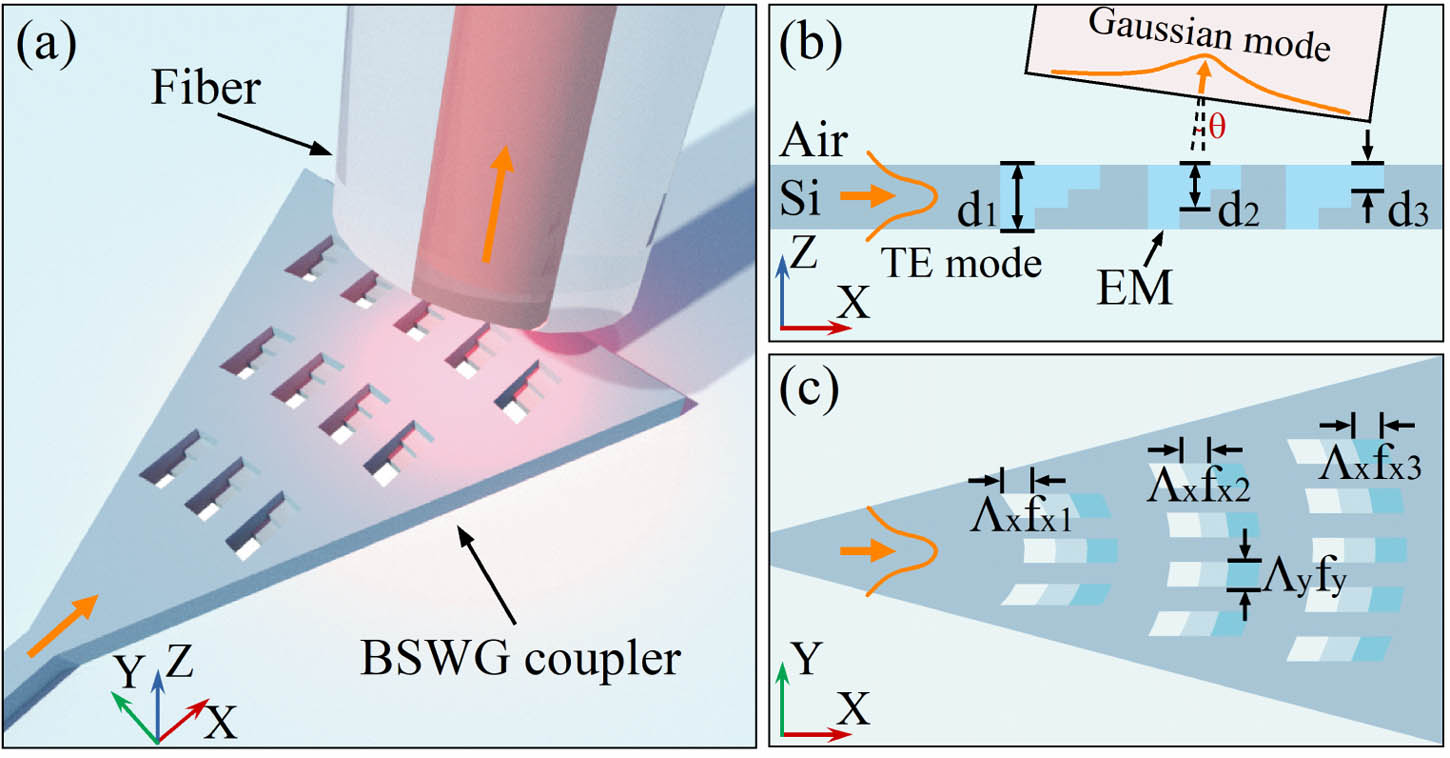
Figure 1.Schematic of the BSWG coupler in (a) 3D view, (b) cross-section view, and (c) top view. BSWGs in the direction can be treated as a homogenous EM when is smaller than the light wavelength.
![Simulation results of SWG couplers. (a) Directionality of uniform BSWG couplers with different parameter combinations of fx and fy. Here, fxa, fxb, and fxc are [0.20, 0.50, 0.15], [0.30, 0.40, 0.15], and [0.40, 0.30, 0.15], respectively. (b) Coupling efficiencies of the single-step-etched SWG coupler, uniform BSWG coupler, and apodized BSWG coupler as a function of wavelength. (c) Grating diffracted electric-field distributions of the single-step-etched SWG coupler (i), uniform BSWG (ii), and apodized BSWG coupler (iii).](/Images/icon/loading.gif)
Figure 2.Simulation results of SWG couplers. (a) Directionality of uniform BSWG couplers with different parameter combinations of and . Here, , , and are [0.20, 0.50, 0.15], [0.30, 0.40, 0.15], and [0.40, 0.30, 0.15], respectively. (b) Coupling efficiencies of the single-step-etched SWG coupler, uniform BSWG coupler, and apodized BSWG coupler as a function of wavelength. (c) Grating diffracted electric-field distributions of the single-step-etched SWG coupler (i), uniform BSWG (ii), and apodized BSWG coupler (iii).
3. FABRICATION AND CHARACTERIZATION OF THE BSWG COUPLER
The grating couplers were fabricated by using an MPW foundry service with a 180-nm CMOS-process line based on an SOI wafer with a 220-nm-thick top silicon layer and a 3-μm-thick buried oxide (BOX) layer. Figures 3(a) and 3(b) show the scanning electron microscope (SEM) images (Thermo Scientific Apreo ) of the uniform and apodized BSWG couplers. As shown in Figs. 3(c) and 3(d), one period of each grating coupler consists of three holes with different colors corresponding to different etch depths of 220 nm, 150 nm, and 70 nm. The corners of the holes are passivated from the square shapes in the grating design to the fabricated oval shapes, due to the limited feature size (180 nm) of the silicon device fabrication in the MPW foundry service. The fabricated errors of the grating structure for different lengths, widths, and etching depths were measured, and the influence of structure deformation on the grating performance was analyzed (see Appendix B). A single-step-etched SWG coupler was also fabricated as a control device. An SEM image of the single-step-etched SWG coupler can be found in Appendix C.
Figure 3.SEM images of uniform and apodized BSWG couplers. (a) Top view of the uniform grating coupler. (b) Top view of the apodized BSWG coupler. (c) Zoom-in image of one period of the uniform BSWG coupler. (d) Zoom-in image of one period of the apodized BSWG coupler.
In the device measurement, an experimental system consisting of an SWMIR continuous-wave single-frequency tunable laser (IPG CLT-2250-500), InGaAs photodiode power meter (Thorlabs S148C), fiber alignment system, and Ge-doped-silica-core optical fibers (Thorlabs SM2000) was used to characterize the performance of the fabricated grating coupler. First, uniform BSWG couplers with different parameter combinations of and were measured. Figure 4(a) shows the performances of uniform BSWG couplers, in which the grating with parameters of of [0.40, 0.30, 0.15] and of 0.5 has the best performance in the experiment. Experimental results show that the BSWG coupler has a maximum coupling efficiency of with a 3-dB bandwidth of at a center wavelength of 2373 nm, which is lower than the simulation result in Fig. 2 due to fabrication errors. We modified the device parameters in the 3D-FDTD simulation model according to the measured structure of the BSWG couplers from the SEM images. In the coupling profile, a noticeable periodic ripple with a free space range (FSR) of 3.9 nm corresponding to Fabry–Perot (F-P) resonance [19] with a cavity length of 165 μm indicates that the uniform BSWG coupler suffers from a large backreflection. Then, the apodized BSWG coupler was measured, which has a great improvement in coupling efficiency, backreflection, as well as spectral bandwidth. As shown in Fig. 4(b), the apodized BSWG coupler has a maximum coupling efficiency of at a center wavelength of 2336 nm and a 3-dB bandwidth of . As a control experiment, we also measured the fabricated single-step-etched SWG coupler, which has a maximum coupling efficiency of only (see Appendix C). Both uniform and apodized BSWG couplers have higher coupling efficiencies than the single-step-etched SWG coupler, indicating that directionality has been significantly improved by using the blazed structure.
Figure 4.Experimental results and 3D-FDTD simulations of uniform and apodized BSWG couplers. (a) Coupling spectrum of the uniform BSWG coupler with of [0.40, 0.30, 0.15] and of 0.5. (b) Coupling spectrum of the apodized BSWG coupler. The maximum coupling efficiency of with the 3-dB bandwidth of was measured at the center wavelength of 2336 nm.
Finally, we studied the optical fiber alignment tolerance and reproducibility of the apodized BSWG coupler, as shown in Fig. 5. Figure 5(a) shows the dependence of coupling efficiency on the incident angle of the optical fiber at different wavelengths. For wavelengths of 2375 nm and 2395 nm, the best incident angle of the apodized BSWG coupler is 10°, consistent with the simulation result, while for a wavelength of 2415 nm, the best incident angle is around 9°, indicating that the center wavelength shifts to longer wavelengths with the decreasing incident angle. Figure 5(b) shows the dependence of coupling efficiency on the optical fiber position in the direction. Since the overlap factor can be changed with the variation of the output mode field diameter (MFD), which is sensitive to the optical fiber position, the coupling efficiency of the apodized BSWG coupler decreases rapidly with the increasing distance between the optical fiber and chip. We also studied the reproducibility of the fabricated apodized BSWG coupler with the same MPW tape-out. Grating couplers in two different dies, namely, die 1 and die 2, with the same design were measured as illustrated in Fig. 5(c). It can be observed that the grating couplers have similar coupling spectra, 3-dB bandwidths, as well as center wavelengths, indicating that the apodized BSWG coupler has excellent reproducibility. Moreover, to expand the working wavelength of the apodized BSWG coupler to the whole SWMIR region, the center wavelength can be shifted by adjusting the grating period. Figure 5(d) shows the coupling efficiency profiles of three grating couplers with different periods of , , and in die 1. Herein, period is the same as that of the design in Fig. 5(c), while and were defined by adding 50 nm to each period of the grating design in Fig. 5(a). Experimental results show that the center wavelength can be tuned from 2336 nm to 2430 nm, while the coupling efficiency has a small deviation of around 0.5 dB.
Figure 5.Optical fiber alignment optimization and reproducibility of the apodized BSWG coupler. (a) Dependence of coupling efficiency on the incident angle of the optical fiber at coupling wavelengths of 2375 nm, 2395 nm, and 2415 nm. (b) Dependence of coupling efficiency (red line) and output MFD (blue line) on the optical fiber position in the direction. Herein, the output MFD was calculated through the Gaussian-shaped beam propagation model. (c) Measurement results of the apodized BSWG coupler with the same design in different dies. (d) Measurement results of the BSWG coupler with different periods of , , and in die 1.
4. CONCLUSION
In conclusion, we demonstrated the BSWG coupler for high-efficiency, wide-bandwidth, and large-tolerance light coupling in the SWMIR band. The apodized BSWG coupler with coupling efficiency of at the center wavelength of 2336 nm with 3-dB bandwidth of was experimentally demonstrated, and is superior to shallowly etched grating, uniform BSWG, and single-step-etched SWG couplers. Moreover, we experimentally studied the best coupling condition and reproducibility of the demonstrated apodized BSWG coupler. Our study is expected to open an avenue toward developing state-of-the-art coupling techniques for SWMIR OEICs based on MPW foundry services.
APPENDIX A: SIMULATION RESULTS OF THE SHALLOWLY ETCHED GRATING COUPLER, SINGLE-STEP-ETCHED SWG COUPLER, AND BSWG COUPLER
We studied the directionality and coupling efficiency of the shallowly etched grating coupler [Figs. 6(a) and 6(b)] and single-step-etched SWG coupler [Figs. 6(c) and 6(d)] by using the 2D-FDTD simulation. Here, the grating couplers were designed based on the SOI wafer with a 220-nm-thick top silicon layer and etching depths of 70 nm, 150 nm, and 220 nm, as well as an SOI wafer with a 340-nm-thick top silicon layer and etching depths of 140 nm, 240 nm, and 340 nm. Figures 6(a) and 6(b) show the simulated results of the shallowly etched grating couplers with different etching depths and different longitudinal fill factors . The shallowly etched grating coupler provides a maximum coupling efficiency of 47% (), while the single-step-etched SWG coupler provides a maximum coupling efficiency of 46% ().
Figure 6.Simulation results of the shallowly etched grating coupler and single-step-etched SWG coupler based on two types of SOI wafers. (a), (b) Directionality and coupling efficiency of the shallowly etched grating coupler based on the SOI wafer with the 220-nm-thick top silicon layer and etching depths of 70 nm, 150 nm, and 220 nm. (c), (d) Directionality and coupling efficiency of the single-etched SWG coupler with of 0.4, 0.5, and 0.6, and of 0.3 based on the SOI wafer with the 220-nm-thick top silicon layer, as well as with of 0.4, 0.5, and 0.6, and of 0.5 based on the SOI wafer with the 340-nm-thick top silicon layer.
Figure 7.Schematics and simulations of the BSWG coupler. (a), (b) Schematics of the uniform BSWG coupler (first four periods) and apodized BSWG coupler (first four periods) in the top view. (c) Theoretical coupling strength and required coupling strength of the apodized BSWG coupler. (d) Directionality and overlap factor of the single-step-etched SWG coupler, uniform BSWG coupler, and apodized BSWG coupler as a function of wavelength. (e), (f) Coupling efficiencies of the single-step-etched SWG coupler, uniform BSWG coupler, and apodized BSWG coupler based on the SOI wafer with the 340-nm-thick top silicon layer for center wavelengths of 2250 and 3200 nm.
APPENDIX B: FABRICATION ERROR ANALYSIS OF THE BSWG COUPLER BASED ON MPW SERVICE
We measured fabrication errors of the BSWG coupler. Figure 8(a) shows the SEM image in the top view of one period of the grating coupler. The designed holes are illustrated as yellow lines, while the fabricated holes are illustrated as blue lines. A schematic of the fabricated holes in the cross-section view is shown in Fig. 8(b). It can be observed that the corners of the holes have been passivated from square shapes to oval shapes, such that the areas of the fabricated holes are smaller than those in the design. Here, the length, width, and depth of the holes are illustrated in Fig. 8(a), and the longitudinal fabrication error and lateral fabrication error are defined as and , respectively. Figure 8(c) shows the dependence of on the widths of the holes with depths of 70 nm, 150 nm, and 220 nm. The measurement shows that the holes with thinner etching depths have larger lateral fabrication errors. Figures 8(d)–8(f) show the dependence of on the lengths of the holes for different widths with depths of 70 nm, 150 nm, and 220 nm, respectively. For the width of 240 nm, the holes with depths of 70 nm could not be fabricated. Moreover, the holes with depths of 150 nm and 220 nm have larger fabrication errors than those with widths of 300 nm and 360 nm. The large fabrication errors could introduce additional loss () and center wavelength shift () in the experiment. It is worthwhile to note that both the width and length of the holes are larger than those of the designs for holes with a depth of 220 nm and width of 360 nm. Last but not least, the overlap misalignment can seriously influence the performance of the grating if the fabrication processes are not stable. According to our experimental results, the MPW service can provide excellent device fabrication reproducibility for the grating design in this study.
Figure 8.Fabrication error analysis of the BSWG coupler. (a) Difference between the designed holes (yellow lines) and fabricated holes (blue lines). (b) Schematic of the fabricated holes in the cross-section view. (c) Dependence of on the widths of the holes with etching depths of 70 nm, 150 nm, and 220 nm. (d)–(f) Dependence of on the lengths of the holes for different widths with etching depths of 70 nm, 150 nm, and 220 nm.
APPENDIX C: CHARACTERIZATION OF THE SINGLE-STEP-ETCHED SWG COUPLER
We designed, fabricated, and measured the single-step-etched SWG coupler in the same MPW tape-out together with the BSWG coupler. Figure 9(a) shows an SEM image of the single-step-etched SWG coupler, which consists of periodically arranged holes with 220-nm etching depth. Figure 9(b) shows experimental results of the single-step-etched SWG coupler, which has the best coupling performance with of 0.5 and of 0.4. The grating coupler has a maximum coupling efficiency of with a 3-dB bandwidth of at a center wavelength of 2350 nm.
Figure 9.Characterization of the single-step-etched SWG coupler. (a) SEM image of the single-step-etched SWG coupler. (b) Experimental measurement of the single-step-etched SWG coupler.
References
[1] M. Xu, M. He, H. Zhang, J. Jian, Y. Pan, X. Liu, L. Chen, X. Meng, H. Chen, Z. Li, X. Xiao, S. Yu, S. Yu, X. Cai. High-performance coherent optical modulators based on thin-film lithium niobate platform. Nat. Commun., 11, 3911(2020).
[2] M. A. Sorokina, S. K. Turitsyn. Regeneration limit of classical Shannon capacity. Nat. Commun., 5, 3861(2014).
[3] S. Zheng, M. Huang, X. Cao, L. Wang, Z. Ruan, L. Shen, J. Wang. Silicon-based four-mode division multiplexing for chip-scale optical data transmission in the 2 μm waveband. Photon. Res., 7, 1030-1035(2019).
[4] W. Cao, D. Hagan, D. J. Thomson, M. Nedeljkovic, C. G. Littlejohns, A. Knights, S.-U. Alam, J. Wang, F. Gardes, W. Zhang, S. Liu, K. Li, M. S. Rouifed, G. Xin, W. Wang, H. Wang, G. T. Reed, G. Z. Mashanovich. High-speed silicon modulators for the 2 μm wavelength band. Optica, 5, 1055-1062(2018).
[5] X. Li, L. Peng, Z. Liu, Z. Zhou, J. Zheng, C. Xue, Y. Zuo, B. Chen, B. Cheng. 30 GHz GeSn photodetector on SOI substrate for 2 μm wavelength application. Photon. Res., 9, 494-500(2021).
[6] R. Soref. Enabling 2 μm communications. Nat. Photonics, 9, 358-359(2015).
[7] X. Liu, B. Kuyken, G. Roelkens, R. Baets, R. M. Osgood, W. M. J. Green. Bridging the mid-infrared-to-telecom gap with silicon nanophotonic spectral translation. Nat. Photonics, 6, 667-671(2012).
[8] R. Soref. Mid-infrared photonics in silicon and germanium. Nat. Photonics, 4, 495-497(2010).
[9] T. Hu, B. Dong, X. Luo, T.-Y. Liow, J. Song, C. Lee, G.-Q. Lo. Silicon photonic platforms for mid-infrared applications [Invited]. Photon. Res., 5, 417-430(2017).
[10] J. Midkiff, K. M. Yoo, J.-D. Shin, H. Dalir, M. Teimourpour, R. T. Chen. Optical phased array beam steering in the mid-infrared on an InP-based platform. Optica, 7, 1544-1547(2020).
[11] R. K. W. Lau, M. R. E. Lamont, Y. Okawachi, A. L. Gaeta. Effects of multiphoton absorption on parametric comb generation in silicon microresonators. Opt. Lett., 40, 2778-2781(2015).
[12] M. Vlk, A. Datta, S. Alberti, H. D. Yallew, V. Mittal, G. S. Murugan, J. Jágerská. Extraordinary evanescent field confinement waveguide sensor for mid-infrared trace gas spectroscopy. Light Sci. Appl., 10, 26(2021).
[13] C. Gu, Z. Zuo, D. Luo, Z. Deng, Y. Liu, M. Hu, W. Li. Passive coherent dual-comb spectroscopy based on optical-optical modulation with free running lasers. PhotoniX, 1, 7(2020).
[14] Y. Yuan, W. V. Sorin, Z. Huang, X. Zeng, D. Liang, A. Kumar, S. Palermo, M. Fiorentino, R. G. Beausoleil. A 100 Gb/s PAM4 two-segment silicon microring resonator modulator using a standard foundry process. ACS Photon., 9, 1165-1171(2022).
[15] A. E. Lim, J. Song, Q. Fang, C. Li, X. Tu, N. Duan, K. K. Chen, R. P. Tern, T. Liow. Review of silicon photonics Foundry efforts. IEEE J. Sel. Top. Quantum Electron., 20, 8300112(2014).
[16] A. Y. Piggott, E. Y. Ma, L. Su, G. H. Ahn, N. V. Sapra, D. Vercruysse, A. M. Netherton, A. S. P. Khope, J. E. Bowers, J. Vučković. Inverse-designed photonics for semiconductor foundries. ACS Photon., 7, 569-575(2020).
[17] Y. Zou, S. Chakravarty, C.-J. Chung, X. Xu, R. T. Chen. Mid-infrared silicon photonic waveguides and devices [Invited]. Photon. Res., 6, 254-276(2018).
[18] X. Xu, H. Subbaraman, J. Covey, D. Kwong, A. Hosseini, R. T. Chen. Complementary metal–oxide–semiconductor compatible high efficiency subwavelength grating couplers for silicon integrated photonics. Appl. Phys. Lett., 101, 031109(2012).
[19] Z. Cheng, X. Chen, C. Y. Wong, K. Xu, H. K. Tsang. Apodized focusing subwavelength grating couplers for suspended membrane waveguides. Appl. Phys. Lett., 101, 101104(2012).
[20] X. Xu, H. Subbaraman, J. Covey, D. Kwong, A. Hosseini, R. T. Chen. Colorless grating couplers realized by interleaving dispersion engineered subwavelength structures. Opt. Lett., 38, 3588-3591(2013).
[21] W. Chen, J. Wu, D. Wan, J. Wang, J. Wang, Y. Zou, Z. Cheng, T. Liu. Grating couplers beyond silicon TPA wavelengths based on MPW. J. Phys. D, 55, 015109(2021).
[22] W. Zhou, H. K. Tsang. Dual-wavelength-band subwavelength grating coupler operating in the near infrared and extended shortwave infrared. Opt. Lett., 44, 3621-3624(2019).
[23] R. Guo, H. Gao, T. Liu, Z. Cheng. Ultra-thin mid-infrared silicon grating coupler. Opt. Lett., 47, 1226-1229(2022).
[24] C. Alonso-Ramos, P. Cheben, A. Ortega-Moñux, J. H. Schmid, D. X. Xu, I. Molina-Fernández. Fiber-chip grating coupler based on interleaved trenches with directionality exceeding 95%. Opt. Lett., 39, 5351-5354(2014).
[25] S. Hong, L. Zhang, Y. Wang, M. Zhang, Y. Xie, D. Dai. Ultralow-loss compact silicon photonic waveguide spirals and delay lines. Photon. Res., 10, 1-7(2022).
[26] X. Chen, D. J. Thomson, L. Crudginton, A. Z. Khokhar, G. T. Reed. Dual-etch apodised grating couplers for efficient fibre-chip coupling near 1310 nm wavelength. Opt. Express, 25, 17864-17871(2017).
[27] P. Cheben, R. Halir, J. H. Schmid, H. A. Atwater, D. R. Smith. Subwavelength integrated photonics. Nature, 560, 565-572(2018).
[28] C. Li, M. Zhang, H. Xu, Y. Tan, Y. Shi, D. Dai. Subwavelength silicon photonics for on-chip mode-manipulation. PhotoniX, 2, 11(2021).
[29] A. Sánchez-Postigo, A. Ortega-Moñux, J. Soler Penadés, A. Osman, M. Nedeljkovic, Z. Qu, Y. Wu, Í. Molina-Fernández, P. Cheben, G. Z. Mashanovich, J. G. Wangüemert-Pérez. Suspended germanium waveguides with subwavelength-grating metamaterial cladding for the mid-infrared band. Opt. Express, 29, 16867-16878(2021).


