1Department of Optics and Optical Engineering, University of Science and Technology of China, Hefei 230026, China
2Key Laboratory of Materials for High-Power Laser, Shanghai Institute of Optics and Fine Mechanics, Chinese Academy of Sciences, Shanghai 201800, China
3Hangzhou Institute for Advanced Study, Chinese Academy of Sciences, Hangzhou 310024, China
Optical physical unclonable functions (PUFs) have emerged as a promising strategy for effective and unbreakable anti-counterfeiting. However, the unpredictable spatial distribution and broadband spectra of most optical PUFs complicate efficient and accurate verification in practical anti-counterfeiting applications. Here, we propose an optical PUF-based anti-counterfeiting label from perovskite microlaser arrays, where randomness is introduced through vapor-induced microcavity deformation. The initial perovskite microdisk laser arrays with regular positions and uniform sizes are fabricated by femtosecond laser direct ablation. By introducing vapor fumigation to induce random deformations in each microlaser cavity, a laser array with completely uneven excitation thresholds and narrow-linewidth lasing signals is obtained. As a proof of concept, we demonstrated that the post-treated laser array can provide fixed-point and random lasing signals to facilitate information encoding. Furthermore, different emission states of the lasing signal can be achieved by altering the pump energy density to reflect higher capacity information. A threefold PUF (excited under three pump power densities) with a resolution of pixels exhibits a high encoding capacity (), making it a promising candidate to achieve efficient authentication and high security with anti-counterfeiting labels.
1. INTRODUCTION
Counterfeiting has become a major challenge in the market, damaging the economy and posing a threat to human health [1–3]. Significant effort has been invested in anti-counterfeiting strategies to address this challenge, especially anti-counterfeiting labels [4–7]. However, conventional anti-counterfeiting labels, such as commonly used graphical barcodes [8] and holograms [9], are not secure because of their deterministic encoding procedures, which can be easily copied. Physical unclonable function (PUF) anti-counterfeiting labels, which are produced by a nondeterministic process, have random physical properties that permit high-complexity and irreproducible code output [10–14]. To date, the optical [15,16], electrical [17], magnetic [18], plasmonic [19], and phase-change features of nanoparticles [20,21] have been adopted in the encoding medium of PUFs. Optical PUFs are the most popular candidates in a variety of coding domains because of their fast readability and easy detection [22–24]. However, because of their uncontrollable growth, several naturally generated optical PUFs are randomly dispersed in spatial locations, making fixed-point detection of the signal difficult.
2D arrays of optical PUFs are expected to resolve the contradiction between high randomness and convenient authentication [10]. Nevertheless, several optical signals, such as random fluorescence patterns [25], have broadband spectra that might even overlap, making distinction difficult and resulting in a low-security level. Compared to broadband fluorescence signals, laser emission has the advantages of extremely narrow linewidth and high irradiance, which makes it easier to distinguish in spectral identification [26,27]. Hence, several laser arrays with variable geometries have been prepared for optical PUFs, including whispering gallery mode (WGM), Fabry–Perot (FP), and random lasers [28–32]. Because of their total internal reflection, the lasing mode of WGM cavities is very sensitive to the geometry of the microcavity [33–35]. Different lasing signals can be achieved by modulating the boundary of the microcavity [36,37], thus promising high-capacity and secure encoding output for anti-counterfeiting labels. If the difference in the lasing modes of WGM lasers with different morphologies can be amplified to increase the accuracy of coding authentication, WGM laser coding might be a promising anti-counterfeiting method.
In this study, we propose an optical PUF-based anti-counterfeiting label from perovskite microlaser arrays, where randomness is introduced via vapor-induced microcavity deformation. WGM microlaser arrays with uniform sizes are fabricated by femtosecond (FS) lasers based on large-scale perovskite thin films. By introducing DMF vapor fumigation, the recrystallization and deformation of the perovskite laser array can be induced. We systematically investigate the influence of deformation on WGM microcavities and the lasing properties of perovskite microlasers. Notably, a laser array with completely uneven excitation thresholds and narrow-linewidth lasing signals is obtained. As a proof of concept, we demonstrated that the treated laser array can provide both fixed-point and random laser signals for laser information encoding. Furthermore, different emission states of the lasing signal can be achieved by altering the pump energy density to reflect higher-capacity information, which is of great significance to achieve efficient authentication and high security for anti-counterfeiting labels.
Sign up for Photonics Research TOC. Get the latest issue of Photonics Research delivered right to you!Sign up now
2. DESIGN PRINCIPLES
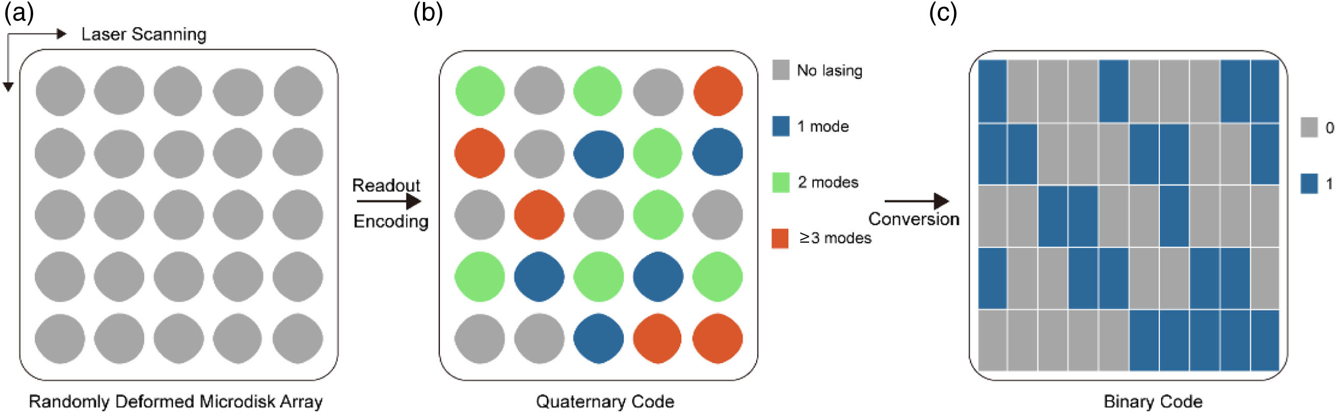
Perovskite single-crystal films are used to fabricate microlaser arrays because of their smooth surface and high optical gain [38]. The most important reason is that by introducing vapor fumigation, defects located at the edge of the perovskite microdisks caused by the machining process will accelerate dissolution and recrystallization [39–42], leading to unpredictable and random deformations in each microlaser cavity. A schematic design principle of the optical PUF label based on a deformed microdisk laser array is illustrated in Fig. 1(a). The slight deformation of the external boundary has a significant effect on the quality factor and resonant frequency of the WGM microcavity, which can be adopted for lasing mode manipulation. By scanning and collecting photoluminescence (PL) emissions, completely uneven lasing signals can be obtained from a well-ordered set of microlaser cavities with different degrees of deformation [Fig. 1(b)], which can be converted into a binary code string according to the distinct lasing mode number [Fig. 1(c)]. Furthermore, because of the dependence of the laser emission on the pump density, the low- resonant mode (higher-order modes) can be amplified, allowing the modulation of the number of lasing modes. Thus, a series of lasing signals in the array may be obtained by increasing the pump density, resulting in a higher-dimensional encoding capability for PUF-based anti-counterfeiting labels.
Figure 1.Schematic design principle of an optical PUF label based on a deformed microdisk laser array. (a) Schematic representation of an optical PUF label ( pixels in this example) based on a deformed microdisk laser array where the randomness was introduced by vapor-induced microcavity deformation. Readout of the PUF label using a confocal PL system by PL mapping and the corresponding digitization of (b) quaternary encoding and (c) binary encoding of the numbers of the lasing peak at each pixel.
A. Fabrication of Perovskite Microdisk Laser Arrays
Appendix A shows the schematic illustration of the growth process of thin film. The chemical vapor method was employed to prepare single-crystal films on freshly cleaved mica substrates. The middle of the tube furnace was filled with cesium bromide (CsBr, 99.99%) and lead bromide (, 99.99%) from Sigma-Aldrich. During growth, 60 sccm high-purity was injected into the tube. The furnace was swiftly heated to 620°C, held for 30 min, and naturally cooled to room temperature. Following the growth, large-scale single-crystal films were obtained on mica surfaces. Direct ablation with second-harmonic (520 nm) 100 kHz laser pulses of a Ti:sapphire laser system was employed to fabricate the perovskite microdisk arrays. The femtosecond (fs) laser power was adjusted to 52 mW and then focused using a dry microscope objective (, NA 0.9, and working distance 3.4 mm).
B. Preparation of Deformed Microdisk Laser Arrays via Vapor Fumigation
The as-prepared circular microdisk arrays were placed on a culture dish and transferred to the top of a hot plate preheated at 90°C in a dry box. A 0.1 mL dimethylformamide (DMF) solution was dropped in the culture plate away from the perovskite and quickly covered with a lid to generate the DMF vapor environment. The samples were fumigated for approximately 10 s before being moved to another hot plate preheated to 250°C and annealed for 10 min in a dry box.
C. Characterizations and Simulation Details
A laser confocal microphotoluminescence system (LabRAM HR Evolution, HORIBA France SAS) and a 400 nm fs-pulsed laser (40 fs, 10 kHz) were used to capture PL and lasing emissions at room temperature. A 400 nm fs laser (repetition rate of 1 kHz, pulse width of 80 fs) equipped with a streak camera (C10910, Hamamatsu) was employed to perform time-resolved PL measurements. SEM was used to characterize the morphology (S-4800, Hitachi). The finite element method (FEM) was employed to study the cavity mode properties, including the electric-field distributions and factor, using a refractive index of 2.3.
D. Digitization of Optical PUF-based Anti-counterfeiting Label
A Python program was designed to extract the digital key and analyze the performance from the lasing data of the PUF labels, which contain both quaternary and binary codes. These are the information processing steps. Three sets of lasing mapping data were imported into the Python program and a corresponding data matrix was generated. A criterion for lasing peak identification was defined: the intensity of the lasing peak should be at least 1.5 times higher than that of the corresponding PL peak. After that, noise reduction and a peak-finding function were applied to extract the number of peaks for each pixel. Based on the number of peaks, quaternary codes were assigned to each pixel: “0” for no lasing, “1” for one lasing peak, “2” for two lasing peaks, and “3” for three or more lasing peaks. Finally, the quaternary codes were converted to binary codes using “1” (white) and “0” (black) as the symbols.
4. RESULTS AND DISCUSSION
A. Fabrication and Characterization of Perovskite Microdisk Array
All-inorganic perovskite was adopted as a gain material to fabricate a laser array because of its better thermal and chemical stability compared to organic-inorganic hybrid perovskites such as [43–45]. The perovskite thin films were synthesized on freshly cleaved mica substrates via an improved vapor deposition method. Figure 2(a) illustrates a schematic of the fabrication of perovskite microdisks via FS laser direct writing, which completely removes the edge of the perovskite microdisks and causes no obvious damage to the remaining microdisks because of their high flexibility, mask-free processing, and nonthermal diffusion. Figure 2(b) illustrates the SEM image of the perovskite microdisks fabricated using the fs laser, which demonstrates an excellent circular microcavity structure and smooth surface. The optical images of the obtained perovskite circular microdisks [Fig. 2(c)] exhibit approximately the same dimensions, demonstrating the robustness of this processing technique. Under UV light excitation, the perovskite microdisk array emits intense green fluorescence, as illustrated in the inset of Fig. 2(c). The as-processed perovskite microdisk array with strong fluorescence and well-defined microdisk morphology provides an excellent foundation for high-performance lasers.
Figure 2.Characterizations and lasing action of the perovskite microdisk array fabricated using a fs laser. (a) Schematic representation of the fabrication processes for a circular microdisk array. (b) SEM image of perovskite microdisks with a diameter of 7 μm. (c) Optical image of the obtained perovskite circular microdisks. Right inset: PL images of perovskite circular microdisks. (d) Excitation power-dependent PL spectra from an individual perovskite microdisk laser. Top inset: schematic of an individual perovskite microdisk laser pumped by a 400 nm laser excitation (, 10 kHz). (e) Dependence of the PL peak intensity and FWHM on the pump density, indicating the evolution from random spontaneous emission to stimulated emission and the lasing threshold at μ. (f) Lorentzian fitting of a lasing mode. The FWHM of the lasing peak is 0.13 nm, corresponding to a factor of .
The laser characteristics of the processed perovskite microdisks were characterized via 400 nm FS laser excitation, as illustrated in the top-left inset of Fig. 2(d). Figure 2(d) illustrates the excitation-power-dependent PL spectra of an individual microdisk laser (with a diameter of 7 μm). A broad PL peak centered at 525 nm is observed at a low power density. When the pump power density exceeds a threshold, a set of sharp peaks emerge at 539.5 nm. Figure 2(e) illustrates the PL peak intensity and FWHM dependence on the pump density, indicating stimulated emission (lasing). When the pump density exceeds μ, the FWHM at is dramatically narrowed, and the PL intensity increases sharply, indicating the evolution from random spontaneous emission to stimulated emission (lasing). The lasing peak at μ is well fitted by a Lorentzian function with an FWHM of 0.13 nm [Fig. 2(f)], demonstrating a high-quality factor of for the processed perovskite microdisks. Hence, perovskite microlaser arrays with excellent lasing performance can be realized using FS laser processing technology.
B. Fabrication and Characterization of Deformed Perovskite Microdisks via Vapor Fumigation
However, because of high-precision FS laser machining technology [46–50], the lasing properties of microlaser arrays are demonstrated to be highly repeatable and robust, as illustrated in Appendix B. To obtain laser arrays with completely different emission spectra, we developed a solvent fumigation post-treatment technique to induce self-repair recrystallization of halide perovskite materials, which can modify the microcavity morphologies and crystallinities, thus modulating the lasing modes, as illustrated in Fig. 3(a). It is worth noting that the FS laser ablation process inevitably introduces a certain degree of vacancy defects at the edges of the microcavity, which can usually be eliminated by annealing. By introducing facile DMF vapor fumigation, defects located at the edge of the perovskite microdisks due to the machining process accelerate the dissolution and recrystallization of the perovskite microcavities. Moreover, different defect densities and vapor concentrations can cause unequal rates of dissolution and recrystallization in each discrete microdisk, and unpredictable and random deformations can also occur in each microlaser cavity. Figure 3(b) illustrates the SEM and optical images of the deformed perovskite microdisk array, which demonstrates periodically distributed microdisks with different morphologies. Under UV light excitation, the deformed perovskite microdisk array also emits strong green fluorescence with significantly brighter deformed boundaries [Fig. 3(b)].
Figure 3.Morphology and optical properties of deformed perovskite microdisk arrays. (a) Schematic representation of the post-treatment processes: (i) FS laser process; (ii) DMF vapor fumigation; and (iii) annealing. (b) SEM and optical images of the deformed perovskite microdisk array, indicating strong green fluorescence and deformed boundaries. (c) Normalized PL spectra of the as-prepared perovskite microdisk with and without vapor fumigation. The PL peak of the perovskite with the vapor fumigation is narrowed (FWHM, ) and blue-shifted. (d) Time-resolved photoluminescence (TR-PL) within the PL lifetime is fitted by a biexponential decay, and the microdisk with post-treatment presents a longer average lifetime (7.43 ns) than the unannealed perovskite (1.47 ns) and unfumigated perovskite microdisks (4.22 ns).
To obtain a deeper understanding of the vapor-induced deformation process, we performed a detailed analysis of the optical properties during recrystallization. Figure 3(c) illustrates the normalized PL spectra of the as-prepared perovskite microdisk with and without vapor fumigation, where the PL peak of the perovskite with vapor fumigation is narrowed (FWHM, ) and blue-shifted, which indicates a narrower distribution of the density of states owing to a reduced defect energy level. The time-resolved photoluminescence (TR-PL) within the PL lifetime is fitted by a biexponential decay owing to two different decay components, as illustrated in Fig. 3(d). The fast decay component () may originate from carrier capture caused by surface defects in the material (Auger or bimolecular recombination process). In contrast, the slow decay () component reflects the carrier lifetime limited by bulk defects in the material. The crystalline quality can be reflected based on average lifetime (), defined as
The as-processed microdisk after FS laser ablation with post-treatment presents a longer average lifetime (7.43 ns) than the unannealed perovskite (1.27 ns) and unfumigated perovskite microdisks (4.22 ns), indicating the enhanced crystalline quality of the vapor-fumigated perovskite microdisks. Therefore, the post-treatment perovskite materials are expected to have a reduced defect density and thus a higher gain to realize lasing output.
C. Theoretical Calculations and Lasing Properties of Deformed Microdisk Cavity
Before studying the lasing properties of the deformed microdisk cavity, theoretical calculations were performed to investigate the influence of cavity deformation on the lasing mode. The film thickness of film is much smaller than the wavelength of the lasing emission. The lasing is unlikely to originate from the Fabry–Perot cavity formed by the top and bottom surfaces of the film, but rather from the WGMs confined by the circular cross-section of the microdisks (Appendix C). In our simulations, the 2D microdisk cavity mode was constructed by FEM, and the refractive index of the deformed microdisks was set to 2.3, which is close to the effective index of films. The deformed microdisk cavity was derived from a circular microdisk with a diameter of 7 μm. We selected simulated resonant frequencies of approximately 557 THz (corresponding to a wavelength of 538 nm) to match the gain of the perovskite material. Figure 4(a) illustrates the simulated field distribution of a deformed microdisk cavity, indicating effective light confinement along the edges and a WGM-like resonant loop. The quality factor ( factor) of the microdisk cavity under different deformations was investigated [Fig. 4(b)]. As the degree of deformation increased, the factor of the microcavity became progressively lower and losses became extreme, implying that more excitation power was required to realize the lasing action. Figure 4(c) illustrates the simulated factors of the microdisk cavity with and without deformation. The circular microdisk cavity has numerous azimuthal modes (cavity modes) in the gain region, and the gain is greater than the loss, which may result in multimode lasing outputs, including fundamental mode lasing and higher-order mode lasing. Compared to a circular microdisk, the number of high- modes in the deformed microdisk is reduced, which may lead to a reduction in the number of lasing modes. Simulation of the resonant mode change as a function of the microdisk deformation is discussed in Appendix D, which indicates a blue shift of resonant wavelengths with finite increasing deformation. Hence, the number of high- resonant modes in the deformed microdisk cavities may depend on cavity deformation.
Figure 4.Cavity mode analysis and lasing action of deformed microdisks. (a) Simulated field distribution of a deformed microdisk cavity indicates effective light confinement along the edges and a WGM-like resonant loop. (b) Quality factor ( factor) of a microdisk cavity indicating the increase in deformation; as the degree of deformation increases, the factor becomes progressively lower. (c) Simulated factors of a microdisk cavity with and without deformation, indicating the decreasing number of high- modes after deformation. (d)–(f) Pseudocolor plot of the pump-density-dependent PL spectra of the deformed perovskite microdisks with different deformations. Insets are the corresponding PL spectra.
We investigated lasing emission by focusing a 400 nm pump laser beam on these deformed microdisks to ensure homogeneous excitation. Taking the three degrees of deformation of perovskite microdisks as examples, Figs. 4(d) and 4(e) illustrate the pseudocolor plot of the pump-density-dependent PL spectra for microdisks with different deformations. The severely deformed microdisk [Sample 1, Fig. 4(d)] consistently has only one lasing-mode peak with increasing laser pump density. Sample 2 consistently exhibits two lasing-mode peaks, as illustrated in Fig. 4(e). However, the slightly deformed microdisk (Sample 3) has only one lasing-mode peak when the pump density is below μ. As the pump density increases, a second lasing peak appears. Once the pump density exceeds μ, extra lasing-mode peaks emerge, which might be attributable to the excitation of higher-order modes in the microcavity. Hence, different deformed microdisks exhibit different lasing peaks, and the number of lasing peaks is strongly dependent on the cavity deformation. Moreover, the integrated PL intensity of the three cavities as a function of pump density is illustrated in Appendix E, which demonstrates that the pump density thresholds are different for different degrees of deformation but of the same order of magnitude (6.1, 9.7, and μ). Therefore, the number of lasing modes and excitation thresholds of the deformed microdisk lasers strongly depend on the cavity deformation.
D. Digitization of the Optical PUF-based Anti-counterfeiting Label Based on Deformed Perovskite Microdisk Array
After completing a detailed study of the lasing properties of randomly selected deformed microdisk lasers, we explored their application potential for anticounterfeit labels. As a proof of concept, we examined the optical performance of a deformed microdisk laser array with an area of μ [Fig. 5(a)] by scanning and measuring the lasing emission of these cavities. In contrast to the disordered naturally grown organic crystals on the substrate, the deformed microdisk arrays exhibit regular position and alignment, which enables maximum integration density and efficient authentication through line-by-line scanning. Figure 5(b-i) illustrates the lasing spectrum of an individual microdisk laser under high-power excitation. The intensity of the lasing peak should simultaneously be 1.5 times higher than that of the corresponding PL peak. We set quaternary encoding rules with four responses per pixel that define no lasing as “0,” one lasing peak as “1,” two lasing peaks as “2,” and three or more lasing peaks as “3.” Therefore, the encoding capacity of a quaternary key with a resolution of pixels is (), which is eight orders of magnitude higher than that of a binary key (), as illustrated in Fig. 5(b-ii). Furthermore, the (25-bit) quaternary keys are converted into a (50-bit) binary key [Fig. 5(b-ii)], achieving a higher spatial density of encoding capacity by increasing the number of possible responses from each pixel. In addition, the same PUF label must be reproducible during repeated authentications. Appendix F illustrates the validation of the same PUF label between the first and second measurements under different pump power intensities. The similarity index of the PUF labels can reach 100%, clearly demonstrating the excellent robustness of the PUF label.
Figure 5.Digitization of the optical PUF-based anti-counterfeiting label. (a) Obtained optical PUF label after post-treatment; pixels are selected as a proof of concept. (b) Digitization of the optical PUF under single-power excitation: (i) lasing spectrum of an individual microdisk laser under high-power excitation, representing four lasing peaks; (ii) quaternary encoding; and (iii) binary encoding of lasing peak numbers at each pixel with a resolution of . (c) Digitization of the optical PUF under variable-power excitation: (i) lasing spectrum of an individual microdisk laser under three power pump densities, the number of lasing peaks increases from one to four; (ii) quaternary encoding and (iii) binary encoding of lasing peak number under three power pump densities at each pixel with a resolution of ; and (iv) combining the threefold binary key into a new PUF label (). (d) Theoretical encoding capacity of an optical PUF label with three encoding methods dependent on the number of pixels , possible responses , and power variations .
To further increase the encoding capacity, we added another encoding dimension. With increasing pump power density, the number of lasing modes of the slightly deformed microdisk laser increases from one to five because of the excitation of relatively low- cavity modes, as illustrated in Fig. 5(c-i). Therefore, the quaternary keys encoded according to the number of laser modes are completely different at different pump power densities and can be used to increase the encoding capacity. Here, we obtained the lasing spectra of a microdisk array at three pump power densities to create a threefold PUF label by following a procedure similar to that described above, as illustrated in Fig. 5(c-ii). The quaternary keys are then converted into a threefold binary key, as shown in Fig. 5(c-iii). Furthermore, the threefold binary key can be combined into a new PUF label () containing threefold coded information, as illustrated in Fig. 5(c-iv). The theoretical encoding capacity of the PUF labels constructed in this manner can be estimated as , where , , and denote the number of lasing peaks, power variations, and pixels, respectively, as shown in Fig. 5(d). The encoding capacity grows exponentially with increasing and and as a power function of . The threefold PUF label with a resolution of pixels has a much larger encoding capacity of (), which is over 30 orders of magnitude larger than the PUF label with the excitation of a single pump power intensity, thus offering greater security of anti-counterfeiting labels. Such a large encoding capacity ensures the impossibility of duplication. Therefore, the results above indicate that optical PUF labels based on deformed microdisk laser arrays may ensure high sampling efficiency and security during certification, making them a promising application for anti-counterfeiting.
5. CONCLUSION
In summary, we proposed an optical PUF-based anti-counterfeiting label from perovskite microlaser arrays, where randomness was introduced through vapor-induced microcavity deformation. We observed that the introduction of DMF vapor fumigation induced the recrystallization and deformation of the uniform perovskite laser array. Random deformation resulted in different quality factors and resonant frequencies of the laser cavity, as proven theoretically. Notably, we obtained a laser array with completely uneven excitation thresholds and narrow-linewidth laser signals. As a proof of concept, we demonstrated that the treated laser array could provide both fixed-point and random laser signals for laser information encoding. Furthermore, different emission states of the lasing signal were achieved by changing the pump energy density to reflect higher-capacity information. A threefold PUF (excited under three pump power densities) with a resolution of exhibited a high encoding capacity (), making it promising to achieve efficient authentication and high security of anti-counterfeiting labels.
Acknowledgment
Acknowledgment. The authors acknowledge the support from the National Natural Science Foundation of China, the Natural Science Foundation of Shanghai, and the Hangzhou Science and Technology Bureau of Zhejiang Province. H.D. acknowledges the Academic/Technology Research Leader Program of Shanghai.
APPENDIX A: SCHEMATIC ILLUSTRATION OF GROWTH PROCESS OF CsPbBr3 THIN FILM
Figure 6 shows the schematic illustration of growth process of single-crystal thin film by the chemical vapor method.
APPENDIX B: REPEATABILITY ANALYSIS OF THE PEROVSKITE MICRODISK ARRAY FABRICATED BY FS LASER
A perovskite microdisk array composed of equal-size disks [μ, Fig. 7(a)] was successfully fabricated by FS laser processing technology. Laser spectra of seven disks above the threshold were captured, and it can be seen from Figs. 7(b) and 7(c) that the lasing modes and thresholds are almost same. The results indicate that the FS laser processing technology could realize high-precision and repeatable fabrication of perovskite microlasers.
Figure 7.Repeatability analysis of the perovskite microdisk array fabricated by FS laser. (a) Optical image of the obtained perovskite circular microdisks with a diameter of 3 μm. (b) Laser spectra of seven equal-size perovskite microdisks. (c) Excitation threshold of seven equal-size perovskite microdisks.
APPENDIX C: INVESTIGATION OF LASING ORIGINS FROM THE THIN-FILM-BASED PEROVSKITE MICRODISK
The film thicknesses of films were measured using atomic force microscopy (AFM). The film thickness was about 150 nm, as shown in Fig. 8(a), which is much smaller than the wavelength of the lasing emission. Moreover, additional simulations were performed to investigate the resonant mode in the 3D microdisk cavity with a diameter μ and a height . Figure 8(b) shows the multi-angle field distribution in the microdisk cavity. The simulation results indicate that electromagnetic fields are confined by the circular cross-section of the microdisks. Therefore, the lasing is unlikely to originate from the Fabry–Perot cavity formed by the top and bottom surfaces of the film, but rather from the whispering gallery modes (WGMs). In addition, the lasing modes are sensitive to the deformation of the microdisk shape, which further supports the WGM origin of the lasing.
Figure 8.Investigation of lasing origins from the thin-film-based perovskite microdisk. (a) AFM image of single-crystal thin film; a typical thickness of 150 nm is determined from the inset profile. (b) 3D-simulated field distribution of the microdisk cavity with a diameter μ and a height .
APPENDIX D: SIMULATION OF THE RESONANT MODE CHANGE AS A FUNCTION OF THE MICRODISK DEFORMATION
A simulation of the resonant mode change was performed as a function of deformation to investigate the effect of vapor-induced randomness. The field distribution of the fundamental mode with an azimuthal number of 72 () is shown in Fig. 9(b), indicating the whispering-gallery-mode-like resonant loop. The corresponding resonant wavelength exhibits a blue shift as the deformation increases [Fig. 9(a)]. Therefore, the calculation results indicate that for this system, an increase in the deformation in the microdisk results in a blue shift of resonant wavelengths with the same azimuthal number.
Figure 9.Simulation of the resonant mode change as a function of the microdisk deformation. (a) Simulated resonant mode of microdisk cavities with increasing deformation, indicating that the corresponding resonant wavelength exhibits a blue shift from 544.12 to 540.71 nm. (b) Simulated field distribution of the fundamental mode with an azimuthal number of 72 ().
Figure 10.Lasing actions from three deformed microdisks. (a)–(c) Power-dependent lasing spectra from three deformed microdisks, respectively. (d) and (e) Integrated emission intensity as a function of pump density showing the lasing threshold at , 9.7, and μ.
APPENDIX E: LASING ACTIONS FROM THREE DEFORMED MICRODISKS
The integrated PL intensity of the three cavities as a function of pump density is illustrated in Fig. 10, which demonstrates that the pump density thresholds are different for different degrees of deformation but of the same order of magnitude (6.1, 9.7, and μ).
APPENDIX F: SIMILARITY STATISTICAL IMAGE OF TWICE MEASUREMENT RESULTS OF THE PUF LABELS
To assess the viability of PUFs, we investigated the readout repeatability of our label, which refers to their ability to produce consistent responses when subjected to repeated identical challenges. Specifically, we analyzed the similarity index of PUF responses obtained from two measurements conducted under high power density conditions, as shown in Fig. 11.