
Qi Yuan, Cuilian Xu, Jinming Jiang, Yongfeng Li, Yang Cheng, He Wang, Mingbao Yan, Jiafu Wang, Hua Ma, Shaobo Qu, "General strategy for ultrabroadband and wide-angle absorbers via multidimensional design of functional motifs," Photonics Res. 10, 2202 (2022)
- Photonics Research
- Vol. 10, Issue 9, 2202 (2022)
Abstract
1. INTRODUCTION
Absorbing electromagnetic (EM) waves in arbitrary directions and polarization has been desired for energy conversion [1–3], EM shielding [4,5], and stealth [6,7] devices in both academia and engineering. By matching the impedance between materials and free space, EM waves can enter materials and then be transformed into other energy [8,9]. There are two typical approaches to design EM absorbers: loss material-based absorbers and structural-based absorbers. Commonly, the loss materials are divided into three types: resistance loss absorption, dielectric loss absorption, and magnetic dielectric loss absorption, which have been utilized to serve the effective absorption in optical, infrared, terahertz and microwave areas [10–22]. While suffering from bulky size, high density, narrowband, or weak resonance, the further development of absorber design is restricted by materials’ inherent drawbacks, especially in broadband and wide angles. As an alternative, the structural resonance-based method is introduced, which achieves the electric or magnetic resonance by meticulous arrangement of the dielectric and metal structure. Particularly, the appearance of metamaterials [23–25], consisting of periodic or quasi-periodic functional motifs, solves the bulky size of the traditional devices and achieves stronger resonance in designed frequency simultaneously, pushing the rapid development EM manipulation as anomalous reflection/deflection [26–28], beam splitting [29–34], RCS reduction [35–38], and holography and imaging [39–44]. Hence, metamaterials have been widely integrated into the study of EM absorbers.
In 2008, Landy
In recent years, intelligent optimization algorithms unveiled the curtain of inverse structure’s design. By endowing codes with corresponding structural parameters, the dimension, size, distribution, and shape of the functional motifs can be encoded into a mathematical expression or computer language. Following the guidance of the preset goal orientation, the performance of designed functional motifs will exceed that of empirical intuition. Till now, the optimization method has achieved perfect performance in broadband absorption [60–64], polarization conversion [65–67], precise wavefront manipulation [68–70], and so on. However, these reported performances would decline sharply with an increase of the incident angle of EM waves. And the mechanism in these works cannot surmount the impedance mismatch problem in broadband and wide angle. Recently, some spatially combined structures have been proposed to improve the angular tolerance of absorption [71,72], yet the research on this issue is still in the nascent stage.
Sign up for Photonics Research TOC. Get the latest issue of Photonics Research delivered right to you!Sign up now
In this work, a general and straightforward strategy is proposed for ultrabroadband and wide-angle absorbers. Theoretically, a spatial combined manner is derived from the analysis of EM wave vectors, reacting to the large and small incident angle by the top and bottom absorbing structure, respectively. Then, a vertical atom sticking on
2. PRINCIPLE AND DESIGN
Figure 1 illustrates the performance of a wide-angle absorber under different EM waves. The proposed functional motifs consist of a vertical atom on
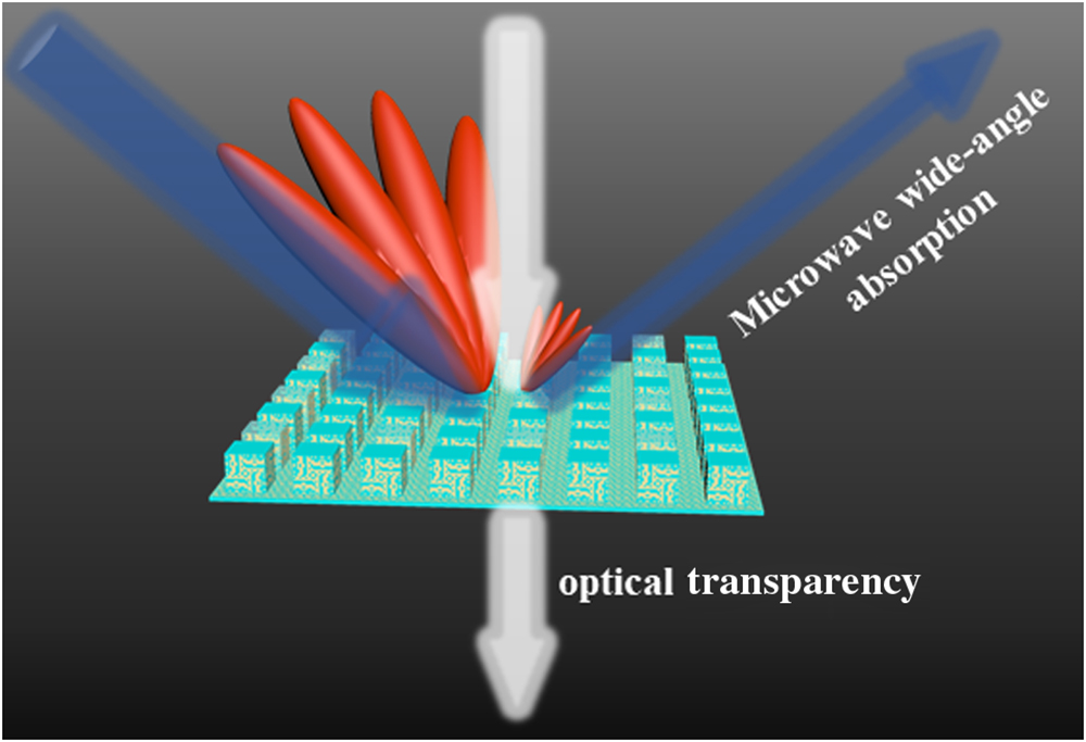
Figure 1.Schematic diagram of the proposed functional motifs with optical transparency and microwave absorption in wide range and broadband.
Figure 2 illustrates the vector decomposition of incident waves. First, we define the direction of normally incident wave as the
![]()
Figure 2.Vector decomposition of incident waves.
To further deduce the reflection coefficient
Figure 3 depicts the mechanism of wide-angle absorption. For small incident angles, the bottom layer serves as the main absorbing layer, which contributes to the strong absorption under the vertical component [Fig. 3(a)]. For large incident angles, the top layer serves as the main absorbing layer, which contributes to the strong absorption under the horizontal component [Fig. 3(b)]. In order to decrease and even eliminate the mutual interference between two orthogonal structures, the intelligent optimization algorithm is introduced to the inverse functional motifs design. To prove the proposed paradigm, the materials with a light transparent characteristic are selected to realize the microwave absorption. As shown in Fig. 4(a), the cubic PMMA substrate (
![]()
Figure 3.Absorbing mechanism of the proposed functional motifs. (a) Small incident angle; (b) large incident angle.
![]()
Figure 4.(a) Functional motifs of the proposed absorber with top, bottom, and back-plane structures, where the square resistance of the ITO back plane is 6 Ω/sq. (b) and (c) are the coding matrix and topology optimization strategy of top and bottom structures, respectively.
In this work, we employ code optimization strategy to design one-eighth of the surface unit, obtaining all the functional motifs by mirror symmetry and central symmetry, where code 0 denotes nothing on the PMMA and code 1 denotes ITO on the PMMA. To get better surface distribution, we set the period gap width of the bottom atom as
The absorption rate is calculated as follows:
The wide-angle absorber optimization design is a multi-objective optimization problem, so the absorbing efficiency, operating frequency band, and angular stability are considered in the fitness calculation function simultaneously. Here, the optimization goal is to achieve maximum operating bandwidth with an absorption rate more than 90% in the frequency range of 2 to 40 GHz and an incidence angle from 0° to 70° concurrently. The fitness function is set as
3. RESULTS AND DISCUSSION
After the joint simulation process, the parameters of the proposed structure are optimized as
![]()
Figure 5.Simulation curves of absorption. Reflection curves of (a) TE and (c) TM waves at 0°, 40°, 60°, and 70°, respectively; absorption characteristics of (b) TE and (d) TM waves from 0° to 80°, respectively.
In order to validate the improvement from the multidimensional design of functional motifs, the absorption of functional motifs, only the top structure and only the bottom structure are discussed in Fig. 6. For both TE and TM polarization waves, the absorptions of top and bottom structures are simulated from 0° to 70°, respectively, and compared with the spatial structure. Figures 6(a)–6(d) showcase each absorption curve of these three structures under TE waves from 0° to 70°. Under small incident angles [Figs. 6(a) and 6(b)], the top structure cannot exhibit strong absorption, while the bottom structure can assist the top structure to improve performance. Under large incident angles [Figs. 6(c) and 6(d)], the top structure has performance very close to the spatial structure, while the absorption of the bottom structure obviously decreases. Figures 6(e)–6(h) showcase each absorption curve of these three structures under TM waves from 0° to 70°. Similar to the results for the TE wave, the top structure shows the strong absorption in the range of large angles, and the bottom structure can assist the top structure to increase the absorption in the range of small angles. Importantly, the absorbing phenomenon of spatial structure has verified our design theme, that the bottom and top structures are utilized to mostly respond to vertical and horizontal waves, respectively (shown in Fig. 3).
![]()
Figure 6.Absorption curves of spatial combined, top, and bottom structures. (a)–(d) Absorption of TE wave at 0°, 40°, 60°, and 70°, respectively; (e)–(h) absorption of TM wave at 0°, 40°, 60°, and 70°, respectively.
To further understand the mechanism of the designed absorber in the range of wide angles, we have monitored the power loss density of the proposed metastructure. Figure 7 shows the energy loss distribution of the strongest resonant peaks under TE and TM waves from 0° to 70°. For incident angle 0°, Fig. 7(a) illustrates the loss distribution of both the top and bottom structures at 8.9 GHz for both TE and TM waves, where most of the energy loss distributes in the horizontal area. For incident angle 40°, Fig. 7(b) depicts the loss distribution at 21.1 GHz for the TE wave and 23.1 GHz for the TM wave, where the energy loss in the horizontal area accounts for a little more than the vertical area around the top structure. Figures 7(a) and 7(b) reveal the fact that the small incident angles have mainly been solved by the bottom structure, which is coherent with our design principle for absorption under small incident angles. For incident angle 60°, Fig. 7(c) showcases the power loss density at 3.4 GHz for the TE wave and 31.3 GHz for the TM waves. With the increase of incident angle, the energy loss in the vertical area around the top structure starts to account for more than in the horizontal area, especially for the TE wave. Meanwhile, the absorption of TE expands to low frequency. For incident angle 70°, Fig. 7(d) displays the loss distribution at 3.5 GHz for the TE wave and 7.1 GHz for the TM wave. In contrast to small incident angles, most of the energy loss distributes in the vertical area, which verifies our proposed design method to absorb EM waves in large incident angles. Moreover, the frequency of resonant peaks varies with incident polarization and angles, revealing the operating mechanism that the broadband polarization-independent absorption is implemented by the coupling of electric and magnetic resonances.
![]()
Figure 7.Loss distribution of different incident angles and polarization at their own maximum resonance peaks. (a) For 0°, both TE and TM at 8.9 GHz; (b) for 40°, TE at 21.1 GHz and TM at 23.1 GHz; (c) for 60°, TE at 3.4 GHz and TM at 31.3 GHz; (d) for 70°, TE at 3.5 GHz and TM at 7.1 GHz.
In addition, the far-field patterns of the designed absorber with
![]()
Figure 8.(a) Simulated 3D far-field patterns under normal incidence at 8, 14, 22, and 28 GHz; (b) simulated monostatic RCS of the designed absorber and group metal from 2 to 40 GHz.
![]()
Figure 9.2D far-field patterns of both absorber and group metal from 4 to 32 GHz in range of 0° to 70° incidences. (a) 0°, (b) 40°, (c) 60°, and (d) 70°. The yellow values mark the value of maximum RCS points, and the range of minimum to maximum is over 25 dB.
To prove the proposed design paradigm and the simulated performance experimentally, a prototype [Fig. 10(a)] with size
![]()
Figure 10.(a) Photograph of the fabricated prototype with the inset showing the functional motifs; (b) experimental setup of mirror reflection measurement; (c) and (d) measured reflection curves of TE and TM waves under 0°, 40°, 60°, and 70° incidences, respectively; (e) measured optical transmittance of the prototype, where red and blue lines represent the transmittance of the red and blue arrow incident types, respectively.
4. CONCLUSION
In summary, a general strategy was proposed for ultrabroadband and wide-angle absorbers via multidimensional design of functional motifs. By coupling the orthogonal meta-atoms, functional motifs exhibit the angular tolerance of impedance matching. To broaden the operating frequency band and maintain angular tolerance simultaneously, an intelligent algorithm is utilized to search the optimal structure parameters. As a demonstration, a wide-angle broadband polarization-independent absorber is designed and verified in microwave regimes. What is more, the proposed functional motifs can be attached with optical transparency function at will, which strongly proves the feasibility of the multidimensional design. We firmly believe that the proposed method can be expanded from microwave to infrared and optical regimes, and the proposed design mentality can be extended to be multispectrum-compatible as an optical hologram and infrared (microwave) stealth-compatible, infrared and microwave stealth-compatible, optical visibility and wavefront manipulation-compatible, etc.
APPENDIX A: OPTIMIZATION STRATEGY OF BROADBAND WIDE-ANGLE IMPEDANCE MATCHING FOR STRONG ABSORPTION IN FULL-POLARIZATION STATES
The main method of optimization is to obtain the optimal parameters of each dimension and surface distribution, respectively, by genetic algorithm (GA), particle swarm optimization (PSO), and so on. In this work, we adopted GA to improve the performance of wide-angle absorption in both TE and TM polarizations. As shown in Fig.
![]()
Figure 11.Flow chart of the joint simulation.
![]()
Figure 12.Coding expression of the structure parameters.
APPENDIX B: MULTIRESONANT ENERGY LOSS DISTRIBUTION IN THE ULTRABROADBAND
To further understand the mechanism of the broadband polarization-independent performance in the range of wide angles, we have monitored the power loss density of the proposed metastructure shown in Fig.
![]()
Figure 13.Power loss density of the proposed functional motifs under different incident angles and polarization at each resonant peak. (a) 0°, (b) 40°, (c) 60°, and (d) 70°.
References
[1] M. M. Ardehali, M. Shahrestani, C. C. Adams. Energy simulation of solar assisted absorption system and examination of clearness index effects on auxiliary heating. Energy Convers. Manage., 48, 864-870(2007).
[2] Q. He, S. Wang, S. Zeng, Z. Zheng. Experimental investigation on photothermal properties of nanofluids for direct absorption solar thermal energy systems. Energy Convers. Manage., 73, 150-157(2013).
[3] Y. Yang, Q. Jin, D. Mao, J. Qi, Y. Wei, R. Yu, A. Li, S. Li, H. Zhao, Y. Ma, L. Wang, W. Hu, D. Wang. Dually ordered porous TiO2-rGO composites with controllable light absorption properties for efficient solar energy conversion. Adv. Mater., 29, 1604795(2017).
[4] D. Chung. Electromagnetic interference shielding effectiveness of carbon materials. Carbon, 39, 279-285(2001).
[5] X. Lu, W. Zhang, C. Wang, T. Wen, Y. Wei. One-dimensional conducting polymer nanocomposites: synthesis, properties and applications. Prog. Polym. Sci., 36, 671-712(2011).
[6] E. F. Knott, J. F. Schaeffer, M. T. Tulley. Radar Cross Section(2004).
[7] H. Mei, D. Yang, L. Yao, W. Yang, X. Zhao, Y. Yao, L. Cheng, L. Zhang, K. G. Dassios. Broadening the absorption bandwidth by novel series–parallel cross convex–concave structures. J. Mater. Chem. C, 9, 5411-5424(2021).
[8] B. Quan, X. Liang, G. Xu, Y. Cheng, Y. Zhang, W. Liu, G. Ji, Y. Du. A permittivity regulating strategy to achieve high-performance electromagnetic wave absorbers with compatibility of impedance matching and energy conservation. New J. Chem., 41, 1259-1266(2017).
[9] C. Song, Y. Huang, P. Carter, J. Zhou, S. Yuan, Q. Xu, M. Kod. A novel six-band dual CP rectenna using improved impedance matching technique for ambient RF energy harvesting. IEEE Trans. Antennas Propag., 64, 3160-3171(2016).
[10] X. Li, C. Wen, L. Yang, R. Zhang, X. Li, Y. Li, R. Che. MXene/FeCo films with distinct and tunable electromagnetic wave absorption by morphology control and magnetic anisotropy. Carbon, 175, 509-518(2021).
[11] P. Liu, S. Gao, G. Zhang, Y. Huang, W. You, R. Che. Hollow engineering to Co@N-doped carbon nanocages via synergistic protecting-etching strategy for ultrahigh microwave absorption. Adv. Funct. Mater., 31, 2102812(2021).
[12] W. Gu, J. Tan, J. Chen, Z. Zhang, Y. Zhao, J. Yu, G. Ji. Multifunctional bulk hybrid foam for infrared stealth, thermal insulation, and microwave absorption. ACS Appl. Mater. Interfaces, 12, 28727-28737(2020).
[13] X. Cui, X. Liang, W. Liu, W. Gua, G. Ji, Y. Du. Stable microwave absorber derived from 1D customized heterogeneous structures of Fe3N@C. Chem. Eng. J., 381, 122589(2020).
[14] Y. Sun, J. Zhang, Y. Zong, X. Deng, H. Zhao, J. Feng, M. He, X. Li, Y. Peng, X. Zheng. Crystalline–amorphous permalloy@iron oxide core–shell nanoparticles decorated on graphene as high-efficiency, lightweight, and hydrophobic microwave absorbents. ACS Appl. Mater. Interfaces, 11, 6374-6383(2019).
[15] E. Nahvi, I. Liberal, N. Engheta. Nonlinear metamaterial absorbers enabled by photonic doping of epsilon-near-zero metastructures. Phys. Rev. B, 102, 035404(2020).
[16] W. Tian, J. Li, Y. Liu, R. Ali, Y. Guo, L. Deng, N. Mahmood, X. Jian. Atomic-scale layer-by-layer deposition of FeSiAl@ZnO@Al2O3 hybrid with threshold anti-corrosion and ultra-high microwave absorption properties in low-frequency bands. Nano-Micro Lett., 13, 161(2021).
[17] Y. Cui, H. Yao, J. Zhang, T. Zhang, Y. Wang, L. Hong, K. Xian, B. Xu, S. Zhang, J. Peng, Z. Wei, F. Gao, J. Hou. Over 16% efficiency organic photovoltaic cells enabled by a chlorinated acceptor with increased open-circuit voltages. Nat. Commun., 10, 2515(2019).
[18] S. Guddala, S. A. Ramakrishna. Optical limiting by nonlinear tuning of resonance in metamaterial absorbers. Opt. Lett., 41, 5150-5153(2016).
[19] S. Saggar, K. D. Deshmukh, S. K. M. McGregor, M. Hasan, A. Shukla, J. S. Agawane, N. Nayak, E. Gann, L. Thomsen, A. Kumar, C. R. McNeill, S. Lo, E. B. Namdas. Impact of polymer molecular weight on polymeric photodiodes. Adv. Opt. Mater., 10, 2101890(2021).
[20] Y. Qiao, Z. Yao, X. Wang, X. Zhang, C. Bai, Q. Li, K. Chen, Z. Li, T. Zheng. Lattice composites with embedded short carbon fiber/Fe3O4/epoxy hollow spheres for structural performance and microwave absorption. Mater. Des., 188, 108427(2020).
[21] S. Guddala, R. Kumar, S. A. Ramakrishna. Thermally induced nonlinear optical absorption in metamaterial perfect absorbers. Appl. Phys. Lett., 106, 111901(2015).
[22] H. Mei, W. Yang, X. Zhao, L. Yao, Y. Yao, C. Chen, L. Cheng. In-situ growth of SiC nanowires@ carbon nanotubes on 3D printed metamaterial structures to enhance electromagnetic wave absorption. Mater. Des., 197, 109271(2021).
[23] J. B. Pendry. Negative refraction makes a perfect lens. Phys. Rev. Lett., 85, 3966-3969(2000).
[24] D. R. Smith, J. B. Pendry, M. C. Wiltshire. Metamaterials and negative refractive index. Science, 305, 788-792(2004).
[25] J. B. Pendry, D. Schurig, D. R. Smith. Controlling electromagnetic fields. Science, 312, 1780-1782(2006).
[26] N. Yu, P. Genevet, M. A. Kats, F. Aieta, J. P. Tetienne, F. Capasso, Z. Gaburro. Light propagation with phase discontinuities: generalized laws of reflection and refraction. Science, 334, 333-337(2011).
[27] X. Ding, F. Monticone, K. Zhang, L. Zhang, D. Gao, S. N. Burokur, A. de Lustrac, Q. Wu, C. Qiu, A. Alù. Ultrathin Pancharatnam-Berry metasurface with maximal cross-polarization efficiency. Adv. Mater., 27, 1195-1200(2015).
[28] S. Sun, K. Yang, C. Wang, T. Juan, W. T. Chen, C. Y. Liao, Q. He, S. Xiao, W. Kung, G. Guo, L. Zhou, D. P. Tsai. High-efficiency broadband anomalous reflection by gradient meta-surfaces. Nano Lett., 12, 6223-6229(2012).
[29] A. Epstein, G. V. Eleftheriades. Synthesis of passive lossless metasurfaces using auxiliary fields for reflectionless beam splitting and perfect reflection. Phys. Rev. Lett., 117, 256103(2016).
[30] Y. Sun, X. Zhang, Q. Yu, W. Jiang, T. J. Cui. Infrared-controlled programmable metasurface. Sci. Bull., 65, 883-888(2020).
[31] W. Guo, G. Wang, X. Luo, H. Hou, K. Chen, Y. Feng. Ultrawideband spin-decoupled coding metasurface for independent dual-channel wavefront tailoring. Ann. Phys., 532, 1900472(2020).
[32] L. Gao, Q. Cheng, J. Yang, S. Ma, J. Zhao, S. Liu, H. Chen, Q. He, W. Jiang, H. Ma, Q. Wen, L. Liang, B. Jin, W. Liu, L. Zhou, J. Yao, P. Wu, T. Cui. Broadband diffusion of terahertz waves by multi-bit coding metasurfaces. Light Sci. Appl., 4, e324(2015).
[33] Y. Pang, Y. Li, B. Qu, M. Yan, J. Wang, S. Qu, Z. Xu. Wideband RCS reduction metasurface with a transmission window. IEEE Trans. Antennas Propag., 68, 7079-7087(2020).
[34] C. Zhang, C. Long, S. Yin, R. Song, B. Zhang, J. Zhang, D. He, Q. Cheng. Graphene-based anisotropic polarization meta-filter. Mater. Des., 206, 109768(2021).
[35] A. Murugesan, D. Natarajan, K. T. Selvan. Low-cost, wideband checkerboard metasurfaces for monostatic RCS reduction. IEEE Antennas Wireless Propag. Lett., 20, 493-497(2021).
[36] Y. Xi, W. Jiang, T. Hong, K. Wei, S. Gong. Wideband and wide-angle radar cross section reduction using a hybrid mechanism metasurface. Opt. Express, 29, 22427-22441(2021).
[37] Q. Zheng, C. Guo, J. Ding, G. A. E. Vandenbosch. A broadband low-RCS metasurface for CP patch antennas. IEEE Trans. Antennas Propag., 69, 3529-3534(2020).
[38] Q. Yuan, H. Ma, J. Jiang, J. Wang, Y. Li, S. Zhao, S. Qu. Al2O3 based ceramic with polarization controlled meta-structure for high-temperature broadband backward scattering manipulation. J. Alloys Compd., 854, 157168(2021).
[39] G. Zheng, H. Mühlenbernd, M. Kenney, G. Li, T. Zentgraf, S. Zhang. Metasurface holograms reaching 80% efficiency. Nat. Nanotechnol., 10, 308-312(2015).
[40] L. Huang, S. Zhang, T. Zentgraf. Metasurface holography: from fundamentals to applications. Nanophotonics, 7, 1169-1190(2018).
[41] Y. Cheng, Y. Li, H. Wang, H. Chen, W. Wan, J. Wang, L. Zheng, J. Zhang, S. Qu. Ohmic dissipation-assisted complex amplitude hologram with high quality. Adv. Opt. Mater., 9, 2002242(2021).
[42] H. Wang, Z. Qin, L. Huang, Y. Li, R. Zhao, H. Zhou, H. He, J. Zhang, S. Qu. Metasurface with dynamic chiral meta-atoms for spin multiplexing hologram and low observable reflection. PhotoniX, 3, 1(2022).
[43] Z. Li, C. Chen, Z. Guan, J. Tao, S. Chang, Q. Dai, Y. Xiao, Y. Cui, Y. Wang, S. Yu, G. Zheng, S. Zhang. Three-channel metasurfaces for simultaneous meta-holography and meta-nanoprinting: a single-cell design approach. Laser Photon. Rev., 14, 2000032(2020).
[44] L. Li, H. Ruan, C. Liu, Y. Li, Y. Shuang, A. Alù, C. Qiu, T. Cui. Machine-learning reprogrammable metasurface imager. Nat. Commun., 10, 1082(2019).
[45] N. I. Landy, S. Sajuyigbe, J. J. Mock, D. R. Smith, W. J. Padilla. Perfect metamaterial absorber. Phys. Rev. Lett., 100, 207402(2008).
[46] Y. J. Yoo, Y. J. Kim, P. V. Tuong, J. Y. Rhee, K. W. Kim, W. H. Jang, Y. H. Kim, H. Cheong, Y. Lee. Polarization-independent dual-band perfect absorber utilizing multiple magnetic resonances. Opt. Express, 21, 32484-32490(2013).
[47] L. Li, Y. Yang, C. Liang. A wide-angle polarization-insensitive ultra-thin metamaterial absorber with three resonant modes. J. Appl. Phys., 110, 063702(2011).
[48] X. Luo, Z. Cheng, X. Zhai, Z. Liu, S. Li, J. Liu, L. Wang, Q. Lin, Y. Zhou. A tunable dual-band and polarization-insensitive coherent perfect absorber based on double-layers graphene hybrid waveguide. Nanoscale Res. Lett., 14, 337(2019).
[49] Z. Zhou, K. Chen, J. Zhao, P. Chen, T. Jiang, B. Zhu, Y. Feng, Y. Li. Metasurface Salisbury screen: achieving ultra-wideband microwave absorption. Opt. Express, 25, 30241-30252(2017).
[50] K. Zhang, X. Cheng, Y. Zhang, M. Chen, H. Chen, Y. Yang, W. Song, D. Fang. Weather-manipulated smart broadband electromagnetic metamaterials. ACS Appl. Mater. Interfaces, 10, 40815-40823(2018).
[51] D. H. Le, S. Lim. Four-mode programmable metamaterial using ternary foldable origami. ACS Appl. Mater. Interfaces, 11, 28554-28561(2019).
[52] Q. Chen, M. Guo, D. Sang, Z. Sun, Y. Fu. RCS reduction of patch array antenna using anisotropic resistive metasurface. IEEE Antennas Wireless Propag. Lett., 18, 1223-1227(2019).
[53] Q. Chen, D. Sang, M. Guo, Y. Fu. Miniaturized frequency-selective rasorber with a wide transmission band using circular spiral resonator. IEEE Trans. Antennas Propag., 67, 1045-1052(2018).
[54] Y. Shen, J. Zhang, Y. Meng, Z. Wang, Y. Pang, J. Wang, H. Ma, S. Qu. Merging absorption bands of plasmonic structures via dispersion engineering. Appl. Phys. Lett., 112, 254103(2018).
[55] L. Zhou, Z. Shen. Absorptive coding metasurface with ultrawideband backscattering reduction. IEEE Antennas Wireless Propag. Lett., 19, 1201-1205(2020).
[56] C. Li, Z. Xu, L. Lin, S. Guo, Y. He, L. Miao, J. Jiang. Ultralow scattering and broadband metasurface using phase adjustable FSS elements embedded with lumped resistors. IEEE Antennas Wireless Propag. Lett., 20, 793-797(2021).
[57] T. Shao, H. Ma, J. Wang, M. Yan, M. Feng, Z. Yang, Q. Zhou, J. Wang, Y. Meng, S. Zhao, S. Qu. Ultra-thin and high temperature NiCrAlY alloy metamaterial enhanced radar absorbing coating. J. Alloys Compd., 832, 154945(2020).
[58] X. Jiang, S. Deng, M. Whangbo, G. Guo. Material research from the viewpoint of functional motifs. Natl. Sci. Rev., 9, nwac017(2022).
[59] M. E. King, M. V. F. Guzmana, M. B. Ross. Material strategies for function enhancement in plasmonic architectures. Nanoscale, 14, 602-611(2022).
[60] S. Jiang, J. Li, J. Li, G. Zhang, H. Liu, F. Yi. Genetic optimization of plasmonic metamaterial absorber towards dual-band infrared imaging polarimetry. Opt. Express, 28, 22617-22629(2020).
[61] J. Chen, W. Ding, X.-M. Li, X. Xi, K. Ye, H. Wu, R. Wu. Absorption and diffusion enabled ultrathin broadband metamaterial absorber designed by deep neural network and PSO. IEEE Antennas Wireless Propag. Lett., 20, 1993-1997(2021).
[62] W. Zhang, H. Qi, Z. Yu, M. He, Y. Ren, Y. Li. Optimization configuration of selective solar absorber using multi-island genetic algorithm. Sol. Energy, 224, 947-955(2021).
[63] H. Zhang, Y. Wang, K. Lu, H. Zhao, D. Yu, J. Wen. SAP-Net: deep learning to predict sound absorption performance of metaporous materials. Mater. Des., 212, 110156(2021).
[64] H. On, L. Jeong, M. Jung, D. Kang, J. Park, H. Lee. Optimal design of microwave absorber using novel variational autoencoder from a latent space search strategy. Mater. Des., 212, 110266(2021).
[65] Q. Yuan, H. Ma, S. Sui, J. Wang, Y. Meng, Y. Pang, S. Qu. A transgenic genetic algorithm design method that helps to increase the design freedom of metasurfaces. J. Phys. D, 54, 135001(2021).
[66] Z. Shi, A. Y. Zhu, Z. Li, Y. Huang, W. Chen, C. Qiu, F. Capasso. Continuous angle-tunable birefringence with freeform metasurfaces for arbitrary polarization conversion. Sci. Adv., 6, eaba3367(2020).
[67] M. Akbari, F. Samadi, A. Sebak, T. A. Denidni. Superbroadband diffuse wave scattering based on coding metasurfaces: polarization conversion metasurfaces. IEEE Antennas Propag. Mag., 61, 40-52(2019).
[68] Q. Ma, G. Bai, H. Jing, C. Yang, L. Li, T. J. Cui. Smart metasurface with self-adaptively reprogrammable functions. Light Sci. Appl., 8, 98(2019).
[69] H. Wang, Y. Jing, Y. Li, L. Huang, M. Feng, Q. Yuan, J. Wang, J. Zhang, S. Qu. Spin-selective corner reflector for retro-reflection and absorption by a circular dichroitic manner. Photon. Res., 9, 726-733(2021).
[70] H. Xu, G. Hu, Y. Wang, C. Wang, M. Wang, S. Wang, Y. Huang, P. Genevet, W. Huang, C. Qiu. Polarization-insensitive 3D conformal-skin metasurface cloak. Light Sci. Appl., 10, 75(2021).
[71] T. Shi, M. Tang, D. Yi, L. Jin, M. Li, J. Wang, C. Qiu. Near-omnidirectional broadband metamaterial absorber for TM-polarized wave based on radiation pattern synthesis. IEEE Trans. Antennas Propag., 70, 420-429(2021).
[72] T. Shi, L. Jin, L. Han, M. Tang, H. Xu, C. Qiu. Dispersion-engineered, broadband, wide-angle, polarization-independent microwave metamaterial absorber. IEEE Trans. Antennas Propag., 69, 229-238(2020).


Set citation alerts for the article
Please enter your email address

© Copyright 2018-2021 | Chinese Laser Press. All Rights Reserved 沪ICP备15018463号-20