• Laser & Optoelectronics Progress
  • Vol. 61, Issue 5, 0504001 (2024)
Qilin Xu1 and Kexue Sun1、2、*
Author Affiliations
  • 1College of Electronic and Optical Engineering & College of Flexible Electronics (Future Technology), Nanjing University of Posts and Telecommunications, Nanjing 210023, Jiangsu , China
  • 2Nation and Local Joint Engineering Laboratory of RF Integration & Micro-Assembly Technology, Nanjing 210023, Jiangsu , China
  • show less
    DOI: 10.3788/LOP230761 Cite this Article Set citation alerts
    Qilin Xu, Kexue Sun. Light Absorption Performance of Graphene Photodetector Based on Localized Surface Plasmon Resonance Effect[J]. Laser & Optoelectronics Progress, 2024, 61(5): 0504001 Copy Citation Text show less
    Model of Si nanowires. (a) 3D model; (b) simplified 2D model
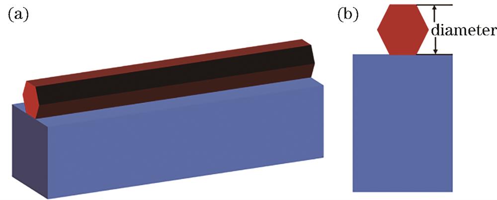
    Fig. 1. Model of Si nanowires. (a) 3D model; (b) simplified 2D model
    Schematic diagram of 2D model. (a) Si nanowire; (b) covering graphene; (c) adding Au grating
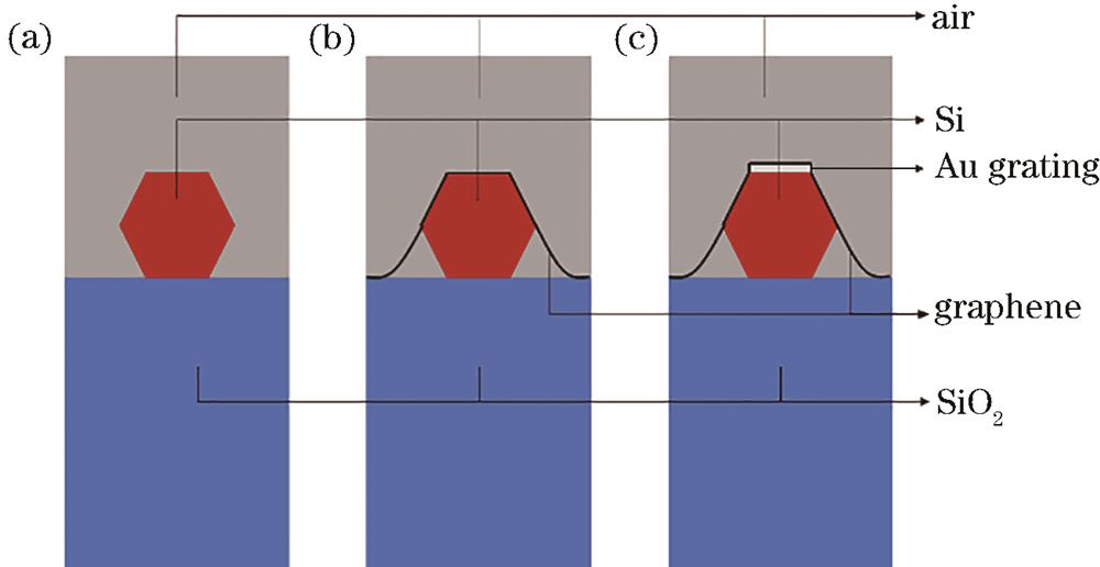
    Fig. 2. Schematic diagram of 2D model. (a) Si nanowire; (b) covering graphene; (c) adding Au grating
    Light absorption curves of device. (a) No covering graphene; (b) covering graphene
    Fig. 3. Light absorption curves of device. (a) No covering graphene; (b) covering graphene
    Comparison of absorption curves of silicon nanowires with diameter of 120 nm with or without graphene
    Fig. 4. Comparison of absorption curves of silicon nanowires with diameter of 120 nm with or without graphene
    Absorption curves of device with different graphene thicknesses
    Fig. 5. Absorption curves of device with different graphene thicknesses
    Curves of device absorption with different thicknesses of Au grating. (a) Au grating thickness is 5 nm; (b) Au grating thickness is 10 nm
    Fig. 6. Curves of device absorption with different thicknesses of Au grating. (a) Au grating thickness is 5 nm; (b) Au grating thickness is 10 nm
    Electric field intensity at the peak of absorption curves for devices with a diameter of 120 nm. (a) Au grating thickness is 5 nm; (b) Au grating thickness is 10 nm
    Fig. 7. Electric field intensity at the peak of absorption curves for devices with a diameter of 120 nm. (a) Au grating thickness is 5 nm; (b) Au grating thickness is 10 nm
    Curves of device absorption with different thicknesses of graphene and Au grating. (a) Au grating thickness is 5 nm; (b) Au grating thickness is 10 nm
    Fig. 8. Curves of device absorption with different thicknesses of graphene and Au grating. (a) Au grating thickness is 5 nm; (b) Au grating thickness is 10 nm
    Qilin Xu, Kexue Sun. Light Absorption Performance of Graphene Photodetector Based on Localized Surface Plasmon Resonance Effect[J]. Laser & Optoelectronics Progress, 2024, 61(5): 0504001
    Download Citation