Abstract
Perovskite light-emitting diodes (PeLEDs) are considered as promising candidates for next-generation solution-processed full-color displays. However, the external quantum efficiencies (EQEs) and operational stabilities of deep-blue (<460 nm) PeLEDs still lag far behind their red and green counterparts. Herein, a rapid crystallization method based on hot-antisolvent bathing is proposed for realization of deep-blue PeLEDs. By promoting immediate removal of the precursor solvent from the wet perovskite films, development of the quasi-two-dimensional (2D) Ruddlesden–Popper perovskite (2D-RPP) crystals with n values >3 is hampered completely, so that phase-pure 2D-RPP films with bandgaps suitable for deep-blue PeLEDs can be obtained successfully. The uniquely developed rapid crystallization method also enables formation of randomly oriented 2D-RPP crystals, thereby improving the transfer and transport kinetics of the charge carriers. Thus, high-performance deep-blue PeLEDs emitting at 437 nm with a peak EQE of 0.63% are successfully demonstrated. The color coordinates are confirmed to be (0.165, 0.044), which match well with the Rec.2020 standard blue gamut and have excellent spectral stability.1 Introduction
Organic–inorganic hybrid perovskite materials have attracted extensive attention in the field of light-emitting diodes (LEDs) as outstanding emitters besides photovoltaics.1–4 Owing to their excellent optoelectronic properties, such as tunable light emission color, high charge-carrier mobility, high photoluminescence (PL) quantum yield (PLQY), and defect tolerance, perovskite LEDs (PeLEDs) have progressed rapidly in terms of performance since their first report in 2014.5–8 At present, green, red, and near-infrared PeLEDs have achieved remarkable external quantum efficiencies (EQEs) of over 20% and exhibited great potential for commercialization in the near future.6,9,10 On the contrary, the development of blue PeLEDs, especially deep-blue PeLEDs with wavelength emissions in the range of 425 to 465 nm, lags far behind those in other spectral regions. Furthermore, the operational stabilities of blue PeLEDs remain as considerable challenges for future exploitation.11,12
Typically, blue emissive PeLEDs have been obtained by adopting two main strategies, namely, crystal size engineering or halide mixing. Blue emissive PeLEDs have been successfully realized with , where blue emission (483 nm) was achieved by reducing the crystal size to within the Bohr radius.13 However, it is difficult to achieve deep-blue emission by only the crystal-size-reducing quantum-confinement effect. Furthermore, undesirable broad electroluminescence (EL) spectra are inevitable owing to uncontrolled crystal size engineering. Instead, halide mixing was suggested as a promising strategy to fabricate deep-blue PeLEDs, where deep-blue emissions were obtained by simply adopting Br-Cl alloyed perovskites.14 Despite its simplicity, light illumination and the applied voltage bias result in halide segregation, causing a severe shift of the EL spectrum to a higher wavelength during operation.15,16 In addition to this spectral instability, the quantum efficiency was significantly limited by the nonradiative decay of charge carriers induced by the halide defects inside the perovskites.
Recently, quasi-two-dimensional (2D) Ruddlesden–Popper perovskites (2D-RPPs) have garnered increasing research interest as alternative materials for blue-emissive PeLEDs.17–23 The 2D-RPPs are derived from conventional three-dimensional (3D) perovskite materials with stoichiometry (where is a univalent small organic cation, is a divalent metal cation, and is a halide ion). Upon introduction of a bulky spacer cation (), the chemical formula of 2D-RPPs can be generally expressed as (), where is the number of inorganic octahedral layers sandwiched between the bulky spacer cations.24 By separating the 3D inorganic octahedral network using bulky spacer cations, blue emissions can be obtained because the bandgaps of the 2D-RPPs broaden with decreasing values. In addition, 2D-RPPs exhibit quantum-well-like electronic properties with strong exciton binding energies owing to the reduced dimensionality, which is beneficial for better PeLED performance.25,26 However, unlike the 3D PeLED application, it is still a challenge to demonstrate blue-emissive and color-pure PeLEDs based on 2D-RPPs, owing to the formation of multiple phases (i.e., various values) during crystallization of the 2D-RPP films.27,28 The main reason for this is the conventional fabrication process, such as hot-casting and the antisolvent dripping method, wherein the bulky spacer cations are spatially segregated during crystallization of the 2D-RPPs, leading to the formation of various perovskite phases with different values.7,29,30 The resulting mixed perovskite phases evoke energy funneling from the perovskite phase with a larger bandgap (i.e., low- phase) to one with a smaller bandgap (i.e., high- phase), thereby causing a significant bathochromic shift and hindering deep-blue emissions.23,24 Therefore, many reports on 2D PeLEDs inevitably utilize Br-Cl alloyed perovskites to enable deep-blue emissions. However, mixed halide compositions still induce halide segregation, which significantly hampers spectral/operational stability.22,31 Consequently, a novel strategy capable of precisely controlling the phase evolution of the 2D-RPP during crystallization is required to achieve spectrally stable deep-blue PeLEDs without halide mixing.
Sign up for Advanced Photonics TOC. Get the latest issue of Advanced Photonics delivered right to you!Sign up now
Herein, we demonstrate deep-blue PeLEDs based on phase-pure 2D-RPPs enabled by a rapid crystallization method. When the as-spin-coated perovskite precursor wet film was submerged in a hot-antisolvent bath of diethyl ether, immediate crystallization occurred because of rapid precursor solvent extraction by the antisolvent. Then, extremely fast crystallization kinetics allowed phenethylammonium (PEA)-based bulky organic spacer cations to be randomly distributed throughout the film, successfully yielding phase-pure 2D-RPP crystals with . Steady-state PL and ultrafast transient absorption (TA) clearly revealed the decent phase purities of the 2D-RPP films in which the generic applicability of the proposed approach was confirmed via various antisolvent candidates. It was also found that randomly oriented perovskite crystals could be obtained during rapid crystallization, facilitating the movement of charge carriers inside the perovskite film. Owing to the enhanced charge transport property, the maximum EQE of deep-blue PeLEDs reached 0.63% with an emission wavelength centered at 437 nm, and the Commission Internationale de l’Eclairage (CIE) coordinates of (0.165, 0.044) were well matched with Rec.2020 standard blue [i.e., CIE chromaticity coordinates of (0.131, 0.046)]. Prolonged stability of the unencapsulated PeLEDs was further achieved with negligibly varying EL spectra during 5 min of operation, which is highly comparable to those of state-of-the-art devices. In this regard, our work proposes a novel approach to realize high-performance spectrally stable deep-blue PeLEDs.
2 Results and Discussion
2.1 Fabrication of 2D-RPP Films
To obtain deep-blue light emissions, the 2D-RPP precursor solution was prepared by mixing PEA bromide, methylammonium bromide, and lead bromide in a molar ratio of 4:1:3 in N-methyl-2-pyrrolidone (NMP) solvent. Using identical perovskite precursor solution, we fabricated 2D-RPP films by either the conventional hot-casting approach or the rapid crystallization method (see the Experimental section for the detailed film deposition process).32–34 Hot-casting, which is considered the most universal fabrication method enabling the fast crystallization kinetic of 2D-RPP films, was chosen as a contrast method.32 The as-spin-coated 2D perovskite precursor wet film was immediately submerged in the antisolvent bath of diethyl ether in the rapid crystallization method. It is well known that the antisolvent extracts the precursor solvent from the wet precursor film via inward diffusion because of their solvent miscibility.35 It is also expected that the remnant precursor solvent would be instantaneously eliminated from the wet film owing to the presence of copious amounts of the antisolvent bath, thereby enabling rapid crystallization of the solute materials. To maximize the solvent extraction speed, we employed a diethyl ether bath in contact with heated water circulator at 40°C, which is above its boiling point to ensure the maximum temperature of antisolvent before evaporation. The 2D perovskite crystallization speeds during both hot-casting and hot-antisolvent bathing were compared by observing the color changes of the resulting perovskite thin films prior to annealing (see Fig. S1 in the Supplementary Material). As shown in the figure, the colorless as-spin-coated film turned yellowish as the nucleation and growth of 2D-RPP crystals progressed. The hot-antisolvent-bathed 2D perovskite film became transparent yellow within , whereas the speed of color change in the case of the hot-cast sample was significantly retarded (). It is noted that the evaporation of the precursor solvent is significantly sluggish owing to the low vapor pressure of NMP (0.342 mm Hg at 25°C) in the case of hot-casting. On the contrary, hot-antisolvent bathing accelerated the 2D perovskite crystallization considerably.
2.2 Morphology and Crystallinity of 2D-RPP Films
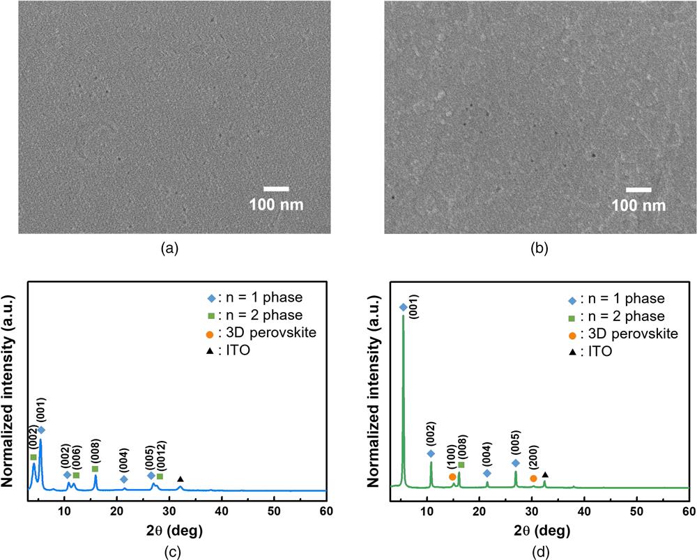
To identify the influences of varying crystallization kinetics on the morphologies of both hot-cast and rapidly crystallized films, scanning electron microscope (SEM) images of the 2D-RPP films deposited on top of poly(3,4-ethylenedioxythiophene):poly(styrene sulfonate) (PEDOT:PSS) were obtained [see Figs. 1(a) and 1(b)]. Both perovskite films exhibited dense and uniform morphologies without any pinholes, as well as similar film thicknesses of according to the cross-sectional SEM images (see Fig. S2 in the Supplementary Material), indicating an insignificant impact of the different crystallization methods on the microstructures of the 2D perovskite films. The surface roughness of both 2D perovskite films was also investigated by atomic force microscopy (see Fig. S3 in the Supplementary Material). Both rapidly crystallized and hot-cast films exhibited highly similar root-mean-square roughness values of 9.33 and 11.53 nm, respectively, indicating an insignificant impact of the different crystallization methods on the microstructures of the 2D perovskite films. X-ray diffraction (XRD) was used to monitor the structural evolutions of both perovskite films after annealing [see Figs. 1(c) and 1(d)]. The XRD pattern of the conventional hot-cast 2D perovskite film clearly shows intense peaks assignable to the (at 5.5 deg, 10.8 deg, and 26.9 deg) and 3D (at 15.1 deg and 30.2 deg) [see Fig. 1(d)].36,37 These results indicate the evolution of the 2D perovskite phases with both low and high -value inside conventional hot-cast 2D-RPP films. By contrast, only diffraction peaks assignable to and 2 perovskite phases were detected in the rapidly crystallized 2D perovskite film. Although the peaks corresponding to the were also observed for the rapidly crystallized 2D perovskite films [see Fig. 1(c)], the hot-cast films showed an approximately sevenfold higher peak intensity of . These observations imply the predominant existence of the perovskite phase in the conventional hot-cast 2D perovskite films compared with the rapidly crystallized films. Meanwhile, the hot-cast film exhibited intensified peaks at 5.5 deg and 10.8 deg, corresponding to the (001) and (002) planes of (i.e., phase) compared to the rapidly crystallized film. It is well known that the 2D perovskite film strongly favors oriented growth parallel to the substrate (e.g., [001] crystal orientations of phase) when fabricated by the conventional hot-casting method,38 similar to that observed in our result. However, it is generally accepted that perovskite thin films comprising randomly oriented crystals enable more efficient charge transport than crystals oriented parallel to the substrate.39,40 This is because of the insulating nature of the 2D spacer cations that block charge-carrier movement along the vertical direction when the crystals are aligned parallel to the substrate, thereby significantly deteriorating device performance.23,41 In contrast, as demonstrated in Fig. 1(c), the hot-antisolvent-bathed film shows nearly negligible intensities of the (001) and (002) plane peaks of the 2D-RPP films, suggesting that the randomly oriented crystals evolve during rapid crystallization, which might be beneficial for fabricating 2D perovskite films for high-efficiency PeLEDs. The random orientation of hot-antisolvent-bathed 2D perovskite crystals was further investigated by grazing incidence XRD (GIXRD) analysis [see Fig. S4 in the Supplementary Material]. As shown in the figure, all the GIXRD patterns collected with different incident angles exhibited negligibly small diffraction peaks of (001) and (002) planes of compared to those of phases, further clearly confirming the scarce amount of phase inside rapidly crystallized 2D perovskite films. Also, it can be observed that the peak intensities of (002) plane of phase and (001) plane of phase abruptly decrease with the increasing incident angle. If the 2D-RPP phases of values 1 and 2 would be grown parallel to the substrate (i.e., spacer cations aligned parallel to the substrate), the intensities of such diffraction peaks should increase with higher incident angles. Therefore, it can be affirmed that the perovskite crystal orientations inside hot-bathed 2D-RPP films are not as parallel compared with the hot-cast films, confirming the random orientation of hot-bathed perovskite crystals. Furthermore, a general area detector diffraction system was utilized for obtaining 2D-XRD profiles of hot-antisolvent-bathed and hot-cast 2D perovskite films to investigate the crystal orientation with respect to the substrate. Note that diffraction patterns with below 10 deg were unobtainable due to the detection limit of the 2D-XRD. As a result, the ring-shaped spectra were successfully observed at 21.4, which can be assigned to the (004) plane of perovskite phase (see Fig. S5 in the Supplementary Material). In contrast, the diffraction patterns corresponding to 3D perovskite (i.e., ) phase were unobservable. The ring-like pattern indicates that the orientations of each perovskite crystals are random relative to each other. Such patterns can be typically observed for the films with polycrystalline grains where they exist as an independent orientational domain. Hence, it can be definitely concluded that rapidly crystallized 2D-RPP films consist of 2D perovskite crystals with random orientation.

Figure 1.Top-view SEM images of (a) rapidly crystallized and (b) conventional hot-cast 2D perovskite films. XRD patterns of 2D-RPP films fabricated with (c) rapid crystallization and (d) conventional hot-casting methods on glass/ITO/PEDOT:PSS (the scale of the axis was adjusted identically for both XRD spectra).
2.3 Phase Evolution of 2D-RPP Films
Next, the phase distribution inside the 2D-RPP films was determined by collecting the PL spectra at a laser excitation wavelength of 325 nm [see Figs. 2(a) and 2(b)]. The PL spectra for the rapidly crystallized film exhibited only two emission peaks at and 437 nm ( and 2 phase peaks, respectively), as shown in Fig. 2(a). It is noted that the intensity of the phase peak at 410 nm is insignificant compared with that of the peak at 437 nm ( times smaller). According to a previous report, the evolution of the phase during crystallization of the 2D perovskite film is inevitable owing to the significantly higher (i.e., negative) formation energy.23 Taking into account this observation, it is speculated that the 2D perovskite film fabricated by rapid crystallization shows outstanding phase purity. In particular, the evolution of the high- perovskite (i.e., ) phase was observed to be completely hampered by the rapid crystallization method. On the contrary, Fig. 2(b) shows the PL spectra for the 2D-RPP films fabricated by the conventional hot-casting method, in which various perovskite phase peaks can be identified. The peaks located at , 437, and 460 nm indicate that 2D-RPP phases with various low- values (i.e., , 2, and 3) co-exist within the film.42 Besides the perovskite phases with low- values, a 3D perovskite (i.e., ) phase peak at was also observed in the PL spectra, as confirmed by the XRD results. This indicates that low- 2D-RPP phases and 3D-like perovskite develop inside the conventional hot-cast 2D perovskite films. As mentioned above, it is noted that the presence of the 3D-like perovskite phase in the film induces energy funneling from low- to high- phase during charge transport, which significantly hinders blue emission. The absorbance spectra of rapidly crystallized and hot-cast 2D-RPP films were also collected (see Fig. S6 in the Supplementary Materials]. It is observed that both the absorption spectra exhibit the peaks corresponding to the 2D perovskite of and 2 (at 404 and 433 nm), respectively. However, the absorption spectra of rapidly crystallized film reveal the intensified peak at 433 nm assignable to the phase, which is in good agreement with the PL results. Also, the broad absorption at around 500 nm can be found in the spectra of hot-cast film, further confirming the existence of high- phases inside the film. To eliminate the influence of the underlying layer on the formation of the phase-pure 2D perovskite film, we additionally assessed the phase purities of 2D-RPP films fabricated on top of either a ZnO or sublayer. As shown in Fig. S7 in the Supplementary Material, the same phase-pure perovskite films consisting of only and 2 phases were confirmed regardless of the type of sublayer used. By contrast, 2D-RPP films prepared by hot-casting still exhibited various PL emission peaks assignable to high- 2D perovskite phases. Therefore, it is concluded that the perovskite film with high phase purity across the entire 2D-RPP film clearly evolved by rapid crystallization.
Figure 2.Steady-state PL spectra of 2D-RPP films fabricated by (a) rapid crystallization and (b) conventional hot-casting approaches on glass/ITO. TA mapping of (c) rapidly crystallized and (d) conventional hot-cast 2D-RPP films with respect to time delays. TA spectra at different time delays of the (e) rapidly crystallized and (f) conventional hot-cast 2D-RPP films.
The PL spectra of the 2D-RPP films bathed in the antisolvent at temperatures lower than 40°C (i.e., 30°C, 20°C, 10°C, and 0°C, respectively) were collected to understand the impact of antisolvent temperature on 2D perovskite phase evolution and hence the formation mechanism of phase-pure 2D perovskite (see Fig. S8 in the Supplementary Material). It is recognized that high- () perovskite phases characterized at wavelengths above 450 nm could form inside the films when bathed in the antisolvent temperature lower than 40°C [see Figs. S8(a) and S8(b) in the Supplementary Material], thus deteriorating the phase purity of the 2D-RPP film. When the antisolvent bath temperature was further reduced to either 10°C or 0°C [see Figs. S8(c) and S8(d) in the Supplementary Material], the intensities of the PL emission peaks corresponding to the high- 2D perovskite phases were further intensified. When the antisolvent bath is at a low temperature, it is speculated that the 2D-RPP crystallization is retarded owing to delayed precursor solvent extraction by the antisolvent, which results in the formation of high- () perovskite phases.43 These observations are in good agreement with the results of the conventional hot-cast 2D perovskite films in which retarded crystallization kinetics induce high- perovskite phases. According to our previous report, retarded crystallization has been found to induce spatial segregation of the bulky spacer cations across the 2D-RPP films owing to the solubility differences between the bulky and small organic cations in the precursor solvent (i.e., NMP).30 In most cases, small organic cations with inferior solubility nucleate first at heterogeneous nucleation sites, yielding 2D perovskite phases with high- values when the perovskite crystallization kinetics is impeded (e.g., 0°C bathing or hot-casting). After the nucleation of the high- perovskite phases, growth of the perovskite crystals incorporates remnant bulky spacer cations, which could lead to the dominant formation of the perovskite phase in the case of conventional hot-cast 2D perovskite films. In contrast, rapid crystallization based on hot-antisolvent bathing induces concurrent incorporation of both organic cations during the entire perovskite crystallization process, resulting in the formation of a phase-pure perovskite with -value of 2 throughout the 2D-RPP film. In this regard, it is confirmed that rapid crystallization driven by fast precursor solvent extraction plays a key role in obtaining highly phase-pure 2D perovskite films.
TA spectroscopy was employed for a better understanding of the phase distributions in the 2D-RPP films. The different phase distributions in the 2D-RPP films fabricated by either conventional hot-casting or hot-antisolvent bathing are clearly revealed by the spectrally and temporally resolved TA mapping excited at a wavelength of 350 nm [see Figs. 2(c) and 2(d)]. The spectra of differential absorptions () at different time delays are presented in Figs. 2(e) and 2(f). TA spectra of the rapidly crystallized 2D-RPP films exhibit ground state bleaching (GSB) peaks at 400 and 430 nm, corresponding to the phases of only and 2 at identical wavelengths as the PL emission peaks [see Fig. 2(c)]. The absence of the perovskite phase with a smaller bandgap (high-) was notable, which is compatible with the PL results. In addition, the intensity of the GSB peak was 4.7 times greater than that of the phase peak, implying the exceptional phase purity of the rapidly crystallized 2D-RPP film [see Fig. 2(e)]. As seen in the TA spectra of the rapidly crystallized 2D-RPP films at different time delays in Fig. 2(e), the reduced GSB signal of the phase at is accompanied by an augmented GSB peak of at , indicating charge transfer from the perovskite phase with a larger to smaller bandgap. This behavior suggests efficient charge transfer from the higher energy phase (low-) to lower energy phase (high-) in the rapidly crystallized 2D-RPP films composed of randomly oriented 2D perovskite crystals, which will be discussed in detail later. For the conventional hot-cast film, in contrast to the rapidly crystallized film, the GSB peaks at 400, 430, 460, and 520 nm (which correspond to the 2D-RPP phases with the value of 1, 2, 3, and , respectively) are identified as shown in Fig. 2(d), which is consistent with the PL results. Therefore, it can be confirmed that uncontrolled spatial arrangement of the bulky spacer cations during perovskite crystallization results in evolution of the various perovskite phases. The GSB peaks successively increased from to in the hot-cast film, indicating funneling of the injected charge carriers toward the 3D-like () perovskite phase. Such energy funneling may inhibit blue emissions and result in green emissions centered at wavelengths over 500 nm.
2.4 Carrier Transfer Kinetics and Defect Analysis
To deeply investigate the carrier transfer process, the time traces of the low- (e.g., and 2) and high- (e.g., ) phases were extracted. The at each wavelength versus time curves are shown in Fig. 3(a) and 3(b). For the rapidly crystallized 2D-RPP film, the GSB peak at 401 nm corresponding to the 2D perovskite phase exhibited the fastest decay kinetics [see Fig. 3(a)]. The intensity of the GSB peak at 401 nm was halved within 10 ps, indicating efficient charge transfer from to higher -value phases. By contrast, the hot-cast 2D-RPP film required over 100 ps for halved GSB peak intensity at 401 nm (i.e., phase) [see Fig. 3(b)]. This observation suggests the sluggish charge transfer kinetics of the hot-cast 2D-RPP film owing to the preferred orientations of the crystals where electrically insulating spacer cations are aligned parallel to the substrate. The GSB peak at 430 nm assignable to the phase of hot-cast film maintained its maximum for about 30 ps. It is speculated that the reduction of the GSB peak of the phase was accompanied by the maintenance of the GSB peak of the phase at 430 nm due to the continuous energy funneling. This behavior implies that the charge transfer occurs from the lower- phases to higher- inside 2D-RPP film. Similarly, the GSB peak at 520 nm corresponding to the phase exhibited the slowest decay, maintaining its maximum even after . This observation was a result of the continuous transfer of charge carriers from the low- (e.g., and 2) to phases for prolonged intervals. The of the GSB peak at 520 nm finally halved after , indicating the steady funneling of charge carriers from low- phases. Consequently, more efficient transfer of the photogenerated charge carriers is observed from the low- to high- phases inside the rapidly crystallized 2D-RPP films than inside the hot-cast 2D perovskite, which is an important prerequisite for fabricating high-performance PeLEDs. For more detailed discussion about TA results, we also compared the normalized TA spectra of both films. As demonstrated in Fig. S9(a), it can be clearly confirmed that the decay of the GSB peak of hot-bathed 2D-RPP film at 401 nm (corresponding to the phase) finished approximately at 1000 ps. Such a decay resulted from the energy funneling of photogenerated carriers to the phase. By contrast, it took more than (i.e., 10,000 ps) for the extinction of the GSB peak of hot-cast 2D-RPP film at 401 nm. It can be also noted that the GSB peaks at 430 and 520 nm, which are assignable for and phases, respectively, exhibit a decay time of over 10 ns. It is speculated that the continuous and elongated funneling of the injected charge carriers results in the sluggish decay of the GSB peaks of and phases. The hot-cast perovskite crystal orientation parallel to the substrate significantly hinders the efficient movement of the charge carriers.
Figure 3.TA kinetics of the (a) rapidly crystallized and (b) conventional hot-cast 2D perovskite films probed at different wavelengths as a function of decay time. Current–voltage curves of hole-only devices fabricated from (c) rapidly crystallized and (d) conventional hot-cast 2D-RPP films obtained under dark conditions using the SCLC method. Hole-only devices in a configuration of glass/ITO/PEDOT:PSS/2D-RPPs/PTAA/Al were utilized.
We performed space-charge-limited current (SCLC) measurements to compare the charge carrier mobilities in the 2D-RPP films fabricated by different methods.44,45 The current–voltage characteristics for hole-only devices in a configuration of glass/indium tin oxide (ITO)/PEDOT:PSS/2D-RPPs/poly[bis(4-phenyl)(2,4,6-trimethylphenyl)amine] (PTAA)/Al are measured as presented in Figs. 3(c) and 3(d). For both cases, the current increased quadratically at high voltages, which is referred to as the Child’s regime. From this region, the hole mobility () of each 2D-RPP film can be calculated by fitting the curve with the Mott–Gurney space-charge model (see the Experimental section for details). The hole mobilities of the rapidly crystallized 2D-RPP films () were calculated to be about 2 orders of magnitude higher than those of the hot-cast 2D perovskite films (). As a result, it can be concluded that the rapid crystallization method effectively enables enhanced charge mobility inside the 2D-RPP films. Such an enhancement mainly originates from the randomly oriented 2D perovskite crystals evolved in the rapidly crystallized 2D-RPP films, as confirmed by TA measurements. The PLQY values of each 2D perovskite film were also measured. It was found that rapidly crystallized 2D-RPP films showed a PLQY of 52%, which is dramatically higher compared to that of the hot-cast film (36%). It is speculated that enhanced transport of charge carrier results in the significantly higher PLQY value. In addition, decreased nonradiative recombination owing to the reduced defect density could contribute to the enhanced PLQY.
The general applicability of the rapid crystallization method was further tested with two additional antisolvent baths (i.e., chlorobenzene and anisole) at 40°C. As exhibited in the XRD spectra of both samples [see Figs. S9(a) and S9(b) in the Supplementary Material], diffraction peaks corresponding to the 3D phase exhibited negligible peak intensities, whereas the peaks corresponding to the phase displayed strong intensities, confirming that the rapid crystallization method is suitable for preparing phase-pure 2D-RPP films regardless of antisolvent types. In addition, the rapid crystallization derived 2D-RPP films obtained with the antisolvent bath of either chlorobenzene or anisole exhibited much weaker (002) diffraction peak of the phase than those of the hot-cast counterpart [see Fig. 1(d)]. This result implies that 2D-RPP films with randomly orientated crystals are readily achieved by bathing the wet precursor films in various antisolvents. The PL spectra of 2D perovskite films prepared by rapid crystallization through bathing in either chlorobenzene or anisole antisolvent were further collected to confirm the perovskite phases evolved inside 2D-RPP films [see Figs. S9(c) and S9(d) in the Supplementary Material]. As demonstrated in the figure, only two peaks, located at 410 and 437 nm, are recognizable regardless of the antisolvent type, corresponding to the perovskite phases of and 2, respectively. The PL emission peaks assignable for 2D perovskite phases with -value of over 3 were unobservable. Therefore, it can be concluded that our proposed rapid crystallization method based on hot-antisolvent bathing is highly suitable for the formation of phase-pure and randomly oriented 2D-RPP films, demonstrating its general applicability to various antisolvent candidates.
2.5 Performance and Stability of 2D PeLEDs Fabricated with Hot-Antisolvent Bathing
Encouraged by the above results, we fabricated the 2D PeLEDs to investigate the effects of the rapid crystallization method on the EL and emission properties. The schematic device configuration and corresponding band energy alignment are presented in Figs. 4(a) and 4(b), respectively. The cross-sectional SEM image of the PeLED structure is displayed in Fig. S11 in the Supplementary Material. As shown in the EL spectra [see Fig. 4(c)], EL peaks were found to be located at 437 nm when the rapidly crystallized 2D-RPP film was employed as the emitter layer for PeLEDs. It is noted that the corresponding EL spectra are in good agreement with the PL spectra of the 2D-RPP film obtained by hot-antisolvent bathing [see Fig. 2(a)]. The EL and emission properties of PeLEDs prepared with the conventional hot-cast 2D perovskite film were also verified (see Fig. S12 in the Supplementary Material). As expected, it is observed that PeLEDs based on the hot-cast 2D perovskite film exhibited green emission, with the main EL peak located at , where only negligible intensities of EL peaks assignable for low- phases can be identified. Such a green emission originates from the funneling of the injected charge carrier from low- perovskite phase toward 3D-like phase owing to the phase evolved inside the 2D-RPP films, confirming the unsuitability of conventional hot-casting for the realization of blue PeLEDs. Also, it is speculated that sluggish transport-driven incomplete funneling of injected charge carriers likely results in the evolution of several emission peaks in the EL spectrum. The performance of the 2D PeLEDs fabricated with the hot-antisolvent bathing-driven 2D-RPP films was further tested as shown in Figs. 4(d) and 4(e). From the luminance ()–voltage () characteristics in Fig. 4(e), the luminance of the PeLED fabricated by the rapid crystallization method steeply increased with voltage, reaching the maximum at . The turn-on voltage (, defined as the voltage at a luminance of ) of the PeLED fabricated by the rapidly crystallized 2D-RPP films was 4.8 V, which is comparable with the values reported for deep-blue emitting 2D PeLEDs. The EQE reached its maximum of 0.63% at a luminance of and current density of , which is comparable to state-of-the-art 2D perovskite thin-film-based deep-blue PeLEDs (see Fig. S13 in the Supplementary Material).22,46 The detailed performance parameters of PeLEDs are summarized in Table 1, and the peak EQE values for 20 individual devices were also collected from four separately prepared batches (see Fig. S14 in the Supplementary Materials). The EQEs of the deep-blue PeLEDs were also compared with the previously reported deep-blue emitting devices fabricated with 2D-RPP thin-films (see Fig. S15 in the Supplementary Material). It should be noted that the performance of our devices is highly comparable with other reports when considering the difficulty of achieving blue LEDs at lower emission wavelength (). The superior performances of the deep-blue devices are mainly attributed to the improved charge transfer and enhanced charge carrier mobility enabled by the randomly oriented crystals inside the rapidly crystallized 2D-RPP films.
Figure 4.(a) Device configuration schematic and (b) band energy alignment of the PeLEDs. EL properties of PeLEDs fabricated from rapidly crystallized 2D perovskite films. (c) EL spectrum under a bias voltage of 6 V. (d) and (e) characteristics.
| Device | () | EL peak (nm) | Max luminance () | EQE (%) | CIE |
| Hot-antisolvent-bathed | 4.8 | 437 | 16.68 | 0.63 | (0.165, 0.044) |
Table 1. Performance parameters of the PeLED prepared from rapidly crystallized 2D-RPP films.
Finally, the operational stabilities of the unencapsulated PeLEDs were evaluated to monitor spectral variations during device operation. As mentioned above, the stability of the PeLED still poses a big challenge, especially for blue PeLEDs, owing to the higher driving voltage compared to their green and red counterparts. It is worth noting that by increasing bias voltage from 5 to 7 V, the EL intensity increased correspondingly, and the EL peak position centered at 437 nm and the full width at half-maximum (FWHM) of 10.8 nm remained unchanged [see Fig. 5(a)]. It can be noted that additional EL peak at around 500 nm started to occur when the bias voltage reached 7 V, indicative of the 2D-RPP film degradation (i.e., the formation of high- phases) due to the high applied bias voltage. When the bias voltage was gradually increased to 9 V, the EL intensity decreased, mainly due to the degradation of the 2D perovskite emission layer (see Fig. S16 in the Supplementary Material). However, both the EL peak position and FWHM remained stable. The stability of the PeLED as a function of the operation time was also investigated, in which the intensity of the EL spectra negligibly changed under continuous operation for 5 min [see Fig. 5(b)], which is highly comparable to other deep-blue PeLEDs reported elsewhere.22,46 The operational lifetime of the PeLEDs was also evaluated by recording the luminance decay under a constant current density at peak EQE, as shown in Fig. S17 in the Supplementary Material. It should be noted that the half-lifetime (i.e., , the time at which the luminance drops to 50% of its initial value) of the PeLEDs fabricated with rapid crystallization was found to be about 10.5 min, which is highly comparable with those of the state-of-the-art deep-blue PeLEDs. As shown in Fig. 5(c), the chromaticity of the fabricated deep-blue PeLEDs exhibited a deep-blue emission with CIE coordinates at (0.165, 0.044), which remarkably accord with the Rec.2020 standard blue color (i.e., ). Figure 5(d) shows the digital photographs of operating PeLEDs in a configuration of glass/ITO/PEDOT:PSS/rapidly crystallized 2D-RPP films/2,2′,2″-(1,3,5-benzinetriyl)-tris(1-phenyl-1-H-benzimidazole) (TPBi)/lithium fluoride (LiF)/Al.
Figure 5.Stability of PeLEDs prepared from rapidly crystallized 2D perovskite films. (a) EL spectra as a function of bias voltage from 5 to 7 V. (b) EL spectra as a function of operation time. The intensities of the EL spectra negligibly changed under continuous operation for 5 min. (c) CIE 1931 chromatic coordinates and (d) digital photograph of the operating device.
3 Conclusion
In this study, we proposed a rapid crystallization method based on hot-antisolvent bathing for fabricating phase-pure 2D perovskite films to realize spectrally stable deep-blue () PeLEDs. By bathing the as-spin-coated 2D perovskite precursor wet film in the hot diethyl ether bath at 40°C, immediate crystallization occurred due to rapid precursor solvent extraction by the antisolvent, yielding phase-pure 2D perovskite crystals. The PL and TA measurements confirmed that the perovskite phase of only with negligible amount of the phase evolved inside the 2D-RPP films, which is highly suitable for preparation of deep-blue-emissive PeLEDs. In contrast, conventional hot-cast 2D perovskite films exhibited various phases, including , 2, 3, and , although an identical precursor solution was utilized, hampering its employment for deep-blue PeLEDs. Furthermore, accelerated crystallization kinetics driven by hot-antisolvent bathing promoted evolution of randomly oriented 2D perovskite crystals, benefiting efficient charge carrier transport inside the 2D-RPP films, as supported by TA and SCLC. Owing to the enhanced charge transport induced by the random orientations of the 2D perovskite crystals, the EQE of the PeLEDs fabricated by the rapidly crystallized 2D perovskite reached 0.63%, which is comparable with that of the thin-film 2D perovskite-based deep-blue PeLEDs reported so far. In addition, our PeLEDs showed outstanding spectral stability without any encapsulation, maintaining both the position and FWHM of the EL peak, even after 5 min of device operation. The color coordinates of the resulting PeLEDs were confirmed to be (0.165, 0.044), which highly satisfy the Rec.2020 standard blue gamut.
Gyumin Jang received his BS degree from the Department of Materials Science and Engineering, Yonsei University, Seoul, Republic of Korea, in 2018. He is currently a PhD student in Yonsei University under the supervision of Professor Jooho Moon. His research has been focused on application of organic-inorganic halide perovskite materials for various optoelectronic devices as well as the chiral perovskite spintronics.
Jooho Moon is a professor in the Department of Materials Science and Engineering at Yonsei University, Seoul, Republic of Korea. He received his MS and PhD degrees in materials science and engineering from the University of Florida. He did his postdoctoral research in the Materials Processing Center at MIT from 1996 to 1998. His research interests include printed electronics and displays, Li ion battery, chiral perovskites, and photoelectrochemical water splitting. He has coauthored more than 270 publications in peer-reviewed journals and he is also serving as an associate editor of ACS Applied Materials & Interfaces since 2015.
Biographies of the other authors are not available.
References
[1] G. Hodes. Perovskite-based solar cells. Science, 342, 317-318(2013).
[2] S. D. Stranks, H. J. Snaith. Metal-halide perovskites for photovoltaic and light-emitting devices. Nat. Nanotechnol., 10, 391-402(2015).
[3] X. Hu et al. High-performance flexible broadband photodetector based on organolead halide perovskite. Adv. Funct. Mater., 24, 7373-7380(2014).
[4] Y. H. Kim et al. Multicolored organic/inorganic hybrid perovskite light-emitting diodes. Adv. Mater., 27, 1248-1254(2015).
[5] Z. K. Tan et al. Bright light-emitting diodes based on organometal halide perovskite. Nat. Nanotechnol., 9, 687-692(2014).
[6] Y. Cao et al. Perovskite light-emitting diodes based on spontaneously formed submicrometre-scale structures. Nature, 562, 249-253(2018).
[7] N. N. Wang et al. Perovskite light-emitting diodes based on solution-processed self-organized multiple quantum wells. Nat. Photonics, 10, 699-704(2016).
[8] Z. G. Xiao et al. Efficient perovskite light-emitting diodes featuring nanometre-sized crystallites. Nat. Photonics, 11, 108-115(2017).
[9] K. B. Lin et al. Perovskite light-emitting diodes with external quantum efficiency exceeding 20 per cent. Nature, 562, 245-248(2018).
[10] T. Chiba et al. Anion-exchange red perovskite quantum dots with ammonium iodine salts for highly efficient light-emitting devices. Nat. Photonics, 12, 681-687(2018).
[11] P. Vashishtha et al. High efficiency blue and green light-emitting diodes using Ruddlesden-Popper inorganic mixed halide perovskites with butylammonium interlayers. Chem. Mater., 31, 83-89(2019).
[12] W. Deng et al. 2D Ruddlesden-Popper perovskite nanoplate based deep-blue light-emitting diodes for light communication. Adv. Funct. Mater., 29, 1903861(2019).
[13] Q. Wang et al. Efficient sky-blue perovskite light-emitting diodes via photoluminescence enhancement. Nat. Commun., 10, 5633(2019).
[14] W. Deng et al. Organometal halide perovskite quantum dot light-emitting diodes. Adv. Funct. Mater., 26, 4797-4802(2016).
[15] S. Draguta et al. Rationalizing the light-induced phase separation of mixed halide organic-inorganic perovskites. Nat. Commun., 8, 200(2017).
[16] G. R. Li et al. Highly efficient perovskite nanocrystal light-emitting diodes enabled by a universal crosslinking method. Adv. Mater., 28, 3528-3534(2016).
[17] Y.-H. Kim et al. Comprehensive defect suppression in perovskite nanocrystals for high-efficiency light-emitting diodes. Nat. Photonics, 15, 148-155(2021).
[18] D. Ma et al. Distribution control enables efficient reduced-dimensional perovskite LEDs. Nature, 599, 594-598(2021).
[19] J. Byun et al. Efficient visible quasi-2D perovskite light-emitting diodes. Adv. Mater., 28, 7515-7520(2016).
[20] D. N. Congreve et al. Tunable light-emitting diodes utilizing quantum-confined layered perovskite emitters. ACS Photonics, 4, 476-481(2017).
[21] Z. W. Ren et al. High-performance blue perovskite light-emitting diodes enabled by efficient energy transfer between coupled quasi-2D perovskite layers. Adv. Mater., 33, 2005570(2021).
[22] G. R. X. Zou et al. Color-stable deep-blue perovskite light-emitting diodes based on organotrichlorosilane post-treatment. Adv. Funct. Mater., 31, 2103219(2021).
[23] J. Xing et al. Color-stable highly luminescent sky-blue perovskite light-emitting diodes. Nat. Commun., 9, 3541(2018).
[24] C. C. Stoumpos et al. Ruddlesden-Popper hybrid lead iodide perovskite 2D homologous semiconductors. Chem. Mater., 28, 2852-2867(2016).
[25] C. H. A. Li et al. The future is blue (LEDs): why chemistry is the key to perovskite displays. Chem. Mater., 31, 6003-6032(2019).
[26] M. Lu et al. Metal halide perovskite light-emitting devices: promising technology for next-generation displays. Adv. Funct. Mater., 29, 1902008(2019).
[27] M. J. Yuan et al. Perovskite energy funnels for efficient light-emitting diodes. Nat. Nanotechnol., 11, 872-877(2016).
[28] L. N. Quan et al. Tailoring the energy landscape in quasi-2D halide perovskites enables efficient green-light emission. Nano Lett., 17, 3701-3709(2017).
[29] S. T. Zhang et al. Efficient red perovskite light-emitting diodes based on solution-processed multiple quantum wells. Adv. Mater., 29, 1606600(2017).
[30] G. Jang et al. Elucidation of the formation mechanism of highly oriented multiphase Ruddlesden-Popper perovskite solar cells. ACS Energy Lett., 6, 249-260(2021).
[31] Y. Shen et al. Interfacial potassium-guided grain growth for efficient deep-blue perovskite light-emitting diodes. Adv. Funct. Mater., 31, 2006736(2021).
[32] H. H. Tsai et al. High-efficiency two-dimensional Ruddlesden-Popper perovskite solar cells. Nature, 536, 312-316(2016).
[33] W. S. Yang et al. High-performance photovoltaic perovskite layers fabricated through intramolecular exchange. Science, 348, 1234-1237(2015).
[34] H. H. Tsai et al. Optimizing composition and morphology for large-grain perovskite solar cells via chemical control. Chem. Mater., 27, 5570-5576(2015).
[35] Y. Y. Zhou et al. Room-temperature crystallization of hybrid-perovskite thin films via solvent-solvent extraction for high-performance solar cells. J. Mater. Chem. A., 3, 8178-8184(2015).
[36] T. L. Leung et al. Mixed spacer cation stabilization of blue-emitting n = 2 Ruddlesden–Popper organic–inorganic halide perovskite films. Adv. Opt. Mater., 8, 1901679(2020).
[37] W. Peng et al. Solution-grown monocrystalline hybrid perovskite films for hole-transporter-free solar cells. Adv. Mater., 28, 3383-3390(2016).
[38] D. H. Cao et al. 2D homologous perovskites as light-absorbing materials for solar cell applications. J. Am. Chem. Soc., 137, 7843-7850(2015).
[39] H. D. Lee et al. Efficient Ruddlesden-Popper perovskite light-emitting diodes with randomly oriented nanocrystals. Adv. Funct. Mater., 29, 1901225(2019).
[40] J. Zhang et al. Uniform permutation of quasi-2D perovskites by vacuum poling for efficient, high-fill-factor solar cells. Joule, 3, 3061-3071(2019).
[41] R. Quintero-Bermudez et al. Compositional and orientational control in metal halide perovskites of reduced dimensionality. Nat. Mater., 17, 900-907(2018).
[42] Y. H. Chang et al. Facile synthesis of two-dimensional Ruddlesden-Popper perovskite quantum dots with fine-tunable optical properties. Nanoscale Res. Lett., 13, 1-7(2018).
[43] G. Jang et al. Cold antisolvent bathing derived highly efficient large-area perovskite solar cells. Adv. Energy Mater., 9, 1901719(2019).
[44] C. Goh et al. Molecular-weight-dependent mobilities in regioregular poly(3-hexyl-thiophene) diodes. Appl. Phys. Lett., 86, 122110(2005).
[45] M. Kiy et al. Observation of the Mott–Gurney law in tris (8-hydroxyquinoline) aluminum films. Appl. Phys. Lett., 80, 1198-1200(2002).
[46] S. Yuan et al. Optimization of low-dimensional components of quasi-2D perovskite films for deep-blue light-emitting diodes. Adv. Mater., 31, 1904319(2019).
[47] J. C. de Mello et al. An improved experimental determination of external photoluminescence quantum efficiency. Adv. Mater., 9, 230-232(1997).
[48] W. Xu et al. In situ-fabricated perovskite nanocrystals for deep-blue light-emitting diodes. J. Phys. Chem. Lett., 11, 10348-10353(2020).
[49] S. Kang et al. Achieving green and deep-blue perovskite LEDs by dimensional control using various ammonium bromides with CsPbBr-3. Mater. Today Energy, 21, 100749(2021).