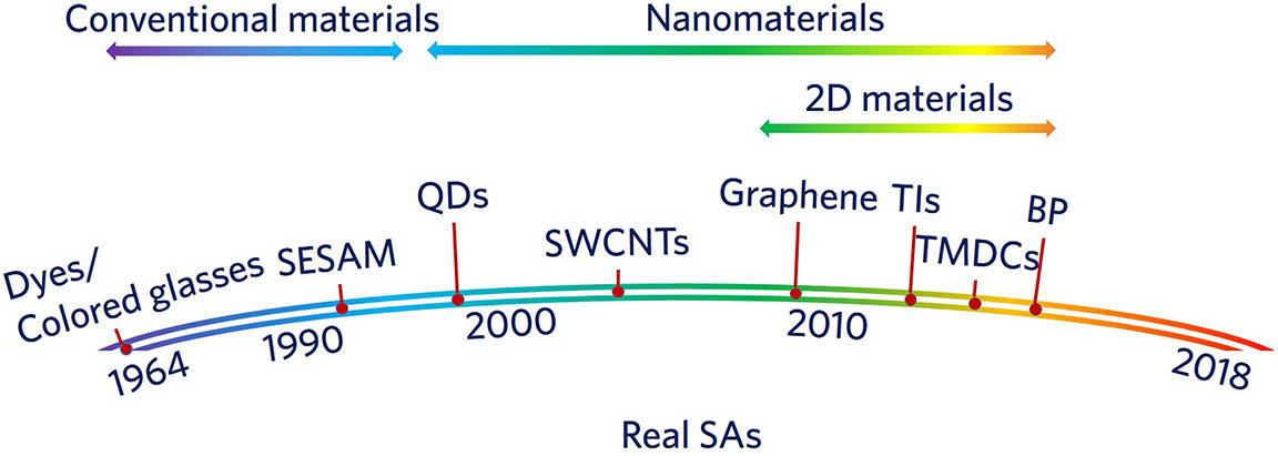
Fig. 1. Evolution of real saturable absorber (SA) technologies starting from conventional materials, such as organic dyes, colored glasses, chromium-doped crystals, and semiconductor SA mirrors (SESAMs), to nanomaterials, including zero-dimensional (0D) quantum dots (QDs), one-dimensional (1D) single-walled carbon nanotubes (SWCNTs), two-dimensional (2D) graphene, and graphene-like 2D layered materials, such as topological insulators (TIs), transition metal dichalcogenides (TMDCs), and black phosphorus (BP). Red dots denote the first, reported application of each technology in a pulsed laser.
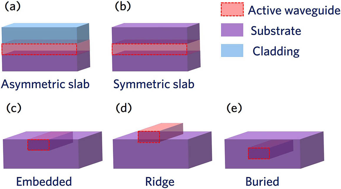
Fig. 2. Schematic diagrams of different types of planar and channel waveguides.
Fig. 3. Common strategies of transferring SA materials on optical substrates on (a) transmitting glass plates, (b) reflecting mirrors, and directly on (c) exposed waveguide surfaces.
Fig. 4. Schematic diagrams of two typical end-pumping configurations of passively Q-switched and mode-locked waveguide lasers based on (a) direct-interaction and (b) evanescent-field-interaction schemes.
Fig. 5. Schematic diagrams of two commonly used strategies for dispersion management in mode-locked waveguide lasers based, respectively, on (a) extended cavities and (b) soliton formation mechanisms realized by adjusting the cavity length, i.e., by tuning the air-filled gap between the SA and waveguide end-facet.
Fig. 6. Figures of merit (FOMs) of pulsed waveguide lasers operating in the Q-switched and Q-switched mode-locked regimes with (a) planar and (b) channel geometries, as well as in (c) the CW mode-locked regime. The FOM errors in these diagrams are ±10%. The symbols’ colors represent waveguide fabrication methods, while the symbols’ appearance stand for different laser configurations in terms of operation regimes, waveguide geometries (circles, Q-switched; triangles, Q-switched mode-locked; squares, planar waveguide lasers operating in the CW mode-locked regime; stars, channel waveguide lasers operating in the CW mode-locked regime) and SA integration types (open markers, free-standing SAs inserted in cavities; filled markers, integrated SAs coated on waveguides).
Fig. 7. Schematic diagram of (a) a hybrid PLD chamber and (b) the graphene-covered
Yb:Y2O3/YAG planar waveguide fabricated by PLD. (c) Measured modal profile of the graphene
Q-switched
Yb:Y2O3/YAG planar waveguide laser. Reproduced with permission from Ref. [
49], ©2015 Optical Society of America.
Fig. 8. (a) Schematic diagram of an LPE arrangement. (b) SEM image of the end-facet of the Tm:KYW/KYW planar waveguide fabricated by LPE. (c) Measured modal profile of the SWCNT
Q-switched Tm:KYW/KYW planar waveguide laser. Reproduced with permission from Ref. [
59], ©2018 Optical Society of America.
Fig. 9. (a) Optical microscope image of the end-facet of the Ho:YAG channel waveguide fabricated by direct bonding. (b) Photograph of the Ho:YAG waveguide sample. (c) Measured modal profile of the Ho:YAG channel waveguide laser. Reproduced with permission from Ref. [
66].
Fig. 10. (a) Schematic diagram of the YAG/RE:YAG/YAG planar waveguide fabricated by tape casting. (b) Measured modal profile of the SESAM mode-locked YAG/Yb:YAG/YAG waveguide laser. Reproduced with permission from Ref. [
69].
Fig. 11. (a) Schematic diagram of mask-assisted ion implantation/irradiation for channel waveguide fabrication. (b) Reconstructed cross-sectional refractive-index distribution of the Nd:YAG channel waveguide fabricated by
C5+ ion irradiation. (c) Measured modal profile of the Nd:YAG channel waveguide laser. Reproduced with permission from Ref. [
72], ©2014 Optical Society of America.
Fig. 12. (a) Cross-sectional TEM image and (b) the superimposed element distribution of the Nd:YAG crystal embedded with Au nanoparticles realized by ion irradiation. The particle size distribution and the nonlinear absorption coefficient at 515 nm of the sample are shown in (c) and (d), respectively. Reproduced with permission from Ref. [
83], ©2018 The Royal Society of Chemistry.
Fig. 13. (a) Schematic diagram of mask-assisted ion exchange for channel waveguide fabrication. (b) Measured modal profile of SESAM mode-locked
Yb3+-doped glass channel waveguide laser fabricated by ion exchange. Reproduced with permission from Ref. [
35], ©2013 Optical Society of America.
Fig. 14. Schematic diagrams of the fabrication procedure of fs-laser-written waveguides
[18]: (a) single-line waveguide based on smooth Type-I modification, (b) stress-induced double-line waveguides based on two parallel Type-II tracks, and (c) depressed-cladding waveguides. The shadows represent the fs-laser-induced tracks, and the dashed lines indicate the spatial locations of the waveguide cores. (d) Schematic diagram of the three-element 3D photonic-lattice-like cladding structures for the
1×4 beam splitter and ring-shaped transformer
[114]. The cross-sectional images of each element are indicated as insets. Reproduced with permission from Ref. [
98], ©2015 SPIE.
Fig. 15. Wavelength ranges covered by solid-state waveguide lasers operating in the CW, Q-switched, Q-switched mode-locked, and CW mode-locked regimes.
| Host Material | Waveguide Type | SA Material | Lasing Wavelength (nm) | Repetition Rate (MHz) | Pulse Duration (ps) | Peak Power (W) | Ref. |
|---|
| External cavity scheme contains free-space optical propagation | | Er/Yb:phosphate glass | Ion-exchanged slab | SESAM | 1545 | 25 | 1.07 | 23.6 | [87] | | Er/Yb:phosphate glass | Ion-exchanged slab | SESAM | 1533.5 | 472 | 6 | 1.6 | [88] | | Er/Yb:phosphate glass | Ion-exchanged slab | SESAM | 1534 | 750 | 6 | 1.6 | [89] | | Er/Yb/Ce:ZBLAN glass | Fs-laser-written cladding | SESAM | 1550 | 156 | 0.18 | 260 | [109] | | Yb:YAG ceramic | Tape-casted sandwich | SESAM | 1030 | 97.79 | 2.95 | 1300 | [69] | | Cr:ZnSe ceramic | Fs-laser-written cladding | SESAM | 2475 | 308.1 | 0.683 | 431 | [110] | | Yb:YAG crystal | Fs-laser-written double-line | SWCNT | 1030.5 | 2080 | 1.89 | 81.9 | [39] | | External cavity scheme contains fiber ring cavity | | Er/Yb:phosphate glass | Fs-laser-written single-line | SWCNT | 1535 | 16.74 | 1.6 | 3.7 | [101] | | Er:bismuthate glass | Fs-laser-written single-line | SWCNT | 1560 | 40 | 0.32 | 97.7 | [102] | | Quasi-monolithic cavity scheme contains an equivalent GTI resonator for soliton formation | | Yb:phosphate glass | Ion-exchanged embedded | SESAM | 1058 | 4926 | 0.74 | 20.7 | [34] | | Er/Yb:phosphate glass | Ion-exchanged embedded | Quantum dot SESAM | 1556 | 6800.3 | 2.5 | 0.8 | [36] | | Yb:phosphate glass | Ion-exchanged embedded | SESAM | 1050 | 15,200 | 0.738 | 8.8 | [35] | | Nd:YAG crystal | Fs-laser-written cladding | Graphene | 1064 | 11,260 | 16.7 | 0.06 | [37,38] | | Ti:sapphire crystal | Fs-laser-written double-line | Graphene | 798.5 | 21,250 | 0.0414 | 122.8 | [40] | | crystal | Fs-laser-written cladding | | 1064 | 6500 | 29 | 1.3 | [111] |
|
Table 1. Summary of the Reported Results for Demonstrations of CW Passively Mode-locked Waveguide Lasers Based on Different Cavity Designs
| Host Material | Waveguide Type | SA Material | Lasing Wavelength (nm) | Repetition Rate (MHz) | Pulse Duration (ps) | Peak Power (W) | Ref. |
|---|
| Quasi-monolithic cavity scheme | | Yb:bismuthate glass | Fs-laser-written single-line | Graphene | 1039 | 1514 | 1.06 | 126 | [103] | | Tm:YAG ceramic | Fs-laser-written cladding | Graphene | 1943.5 | 7800 | – | – | [104] | | Er/Yb:phosphate glass | Ion-exchanged embedded | Graphene | 1535 | 6800 | 6 | 0.66 | [90] | | Ho:YAG crystal | Fs-laser-written cladding | Graphene | 2091 | 5900 | – | 1600 | [105] | | crystal | Fs-laser-written cladding | Graphene, , | 1064 | 6436–6556 | 26–52 | 1.1–1.6 | [106] | | crystal | Fs-laser-written cladding | Nanoparticle-modified graphene | 1064 | 6440 | 33 | 0.7 | [84] | | crystal | Fs-laser-written cladding | Nanoparticle-modified | 1064 | 6400 | 74.1 | – | [85] | | External cavity scheme contains free-space optical propagation | | Tm:ZBLAN glass | Fs-laser-written cladding | Graphene, CNT, , , , , , BP, ITO | 1865–1880 | 436 | – | – | [107,108] |
|
Table 2. Summary of the Reported Results for Demonstrations of Passively Q-switched Mode-locked Waveguide Lasers Based on Different Cavity Designs
| Host Material | Waveguide Type | SA Material | Interaction Scheme | Lasing Wavelength (nm) | Repetition Rate (MHz) | Pulse Duration (ns) | Peak Power (W) | Ref. |
|---|
| Organic-dye-based SAs | | Nd:phosphate glass | Ion-exchanged embedded | BDN | Transmission | 1054 | 0.05 | 20 | 3.04 | [9] | | Nd:phosphate glass | Ion-exchanged embedded | BDN | Evanescence field | 1054 | 0.35 | 10 | 1 | [30] | | Nd:phosphate glass | Ion-exchanged embedded | BDN | Evanescence field | 1053 | 0.028 | 1.3 | 1000 | [91] | | Yb:phosphate glass | Ion-exchanged embedded | BDN | Evanescence field | 1030 | 0.021 | 12 | 3 | [92] | | Cr-doped crystal-based SAs | | Nd:YAG crystal | Contact-bonded sandwich | Cr:YAG | Transmission | 1064 | 0.08 | 2.5 | 28,000 | [64] | | Yb:YAG crystal | Contact-bonded sandwich | Cr:YAG | Transmission | 1030 | 0.077 | 1.6 | 18,000 | [65] | | Nd:YAG ceramic | Fs-laser-written cladding | Cr:YAG | Transmission | 1064 | 0.0344 | 2.8 | 7000 | [32] | | Nd:YAG crystal | Fs-laser-written cladding | Cr:YAG | Transmission | 1064 | 0.0719 | 3.9 | 4000 | [33] | | Tm:KYW crystal | LPE-grown sandwich | Cr:ZnSe | Transmission | 1844.7 | 0.010 | 1200 | 0.1 | [57] | | Ho:YAG crystal | Contact-bonded buried | Cr:ZnSe | Reflection | 2091 | 0.442 | 1000 | 1 | [66] | | crystal | Fs-laser-written double-line | – | Self--switching | 1064 | 2.3 | 85 | 0.3 | [31] | | Nd:YAG ceramic | Fs-laser-written cladding | Cr:YAG | Transmission | 1064 | 0.067 | 4 | 1950 | [127] | | crystal | Fs-laser-written cladding | Cr:YAG | Transmission | 1064 | 0.083 | 6.8 | 1360 | [127] | | Semiconductor-based SAs | | Yb:KYW crystal | LPE-grown slab | SESAM | Reflection | 1040 | 0.772 | 170 | 0.3 | [54] | | Nd:YAG ceramic | Fs-laser-written double-cladding | SESAM | Reflection | 1064 | 3.65 | 21 | 0.6 | [112] | | Yb:YAG crystal | Fs-laser-written double-line | SESAM | Reflection | 1030 | 5.4 | 11 | 91 | [41] | | crystal | Ion-implanted slab | GaAs | Transmission | 1063.6 | 0.0294 | 3.88 | 212 | [71] | | SWCNT-based SAs | | Yb:KYW crystal | LPE-grown slab | SWCNT | Evanescence field | 1030 | 0.241 | 433 | 0.3 | [55] | | Yb:YAG crystal | Fs-laser-written double-line | SWCNT | Reflection | 1029 | 1.59 | 78 | 0.5 | [115] | | Tm:KYW crystal | LPE-grown slab | SWCNT | Reflection | 1835.4 | 1.39 | 83 | 0.4 | [59] | | Tm:KLW crystal | Fs-laser-written cladding | SWCNT | Evanescence field | 1844-1847.9 | 2.2 | 90 | 1.1 | [128] | | Graphene-based SAs | | Yb:phosphate glass | Ion-exchanged embedded | Graphene | Reflection | 1057 | 0.833 | 140 | 0.2 | [90] | | crystal | Fs-laser-written cladding | Graphene | Reflection | 1064 | 17.8 | 79 | 0.3 | [116] | | Nd:YAG crystal | Fs-laser-written cladding | Graphene | Reflection | 1064 | 4 | 70 | 0.8 | [114] | | Nd:YAG crystal | Fs-laser-written cladding | Graphene | Evanescence field | 1064 | 10.4 | 52 | 0.1 | [117] | | Nd:YAG crystal | Fs-laser-written Y-branch | Graphene | Reflection | 1064 | 3 | 90 | 0.7 | [113] | | Nd:YAG crystal | Fs-laser-written Y-branch | Graphene | Evanescence field | 1064 | 2.3 | 200 | 0.3 | [113] | | crystal | Fs-laser-written multi-line | Graphene | Reflection | 1064 | 16.3 | 25 | 0.3 | [118] | | Yb:YAG crystal | Fs-laser-written double-line | Graphene | Reflection | 1029 | 1.33 | 79 | 0.7 | [28] | | Nd:YAG ceramic | Tape-casted sandwich | Graphene oxide | Reflection | 1064 | 0.93 | 179 | 1.2 | [70] | | crystal | PLD | Graphene | Reflection | 1030.8 | 1.04 | 98 | 0.1 | [48] | | crystal | PLD | Graphene | Evanescence field | 1030 | 1.64 | 124 | 2.5 | [49] | | Yb:KYW crystal | LPE-grown slab | Graphene | Evanescence field | 1027 | 0.607 | 349 | 0.2 | [56] | | Nd:YAG ceramic | Ion-irradiated embedded | Graphene | Transmission | 1064 | 4.1 | 57 | 1.4 | [72] | | Nd:YAG crystal | Ion-irradiated slab | Graphene | Evanescence field | 1064 | 0.029 | 9800 | 0.04 | [73] | | Nd:YAG crystal | Ion-irradiated ridge | Graphene | Transmission | 1064 | 4.2 | 90 | 0.3 | [74] | | Nd:YAG crystal | Ion-irradiated slab | Graphene | Evanescence field | 1064 | 2 | 32 | 0.3 | [78] | | Tm:KYW crystal | LPE-grown sandwich | Graphene | Transmission | 1831.8 | 1.13 | 195 | 0.03 | [58] | | Nd:YAG crystal | Ion-irradiated slab | Ion-beam modified graphene | Transmission | 1064 | 2.3 | 101 | 0.03 | [81] | | crystal | Fs-laser-written cladding | Graphene | Transmission | 1064 | 7.8 | 22 | 0.9 | [123] | | crystal | Fs-laser-written cladding | Graphene | Transmission | 1064 | 8.897 | 55 | 0.5 | [125] | | Yb, crystal | Fs-laser-written double-line | Graphene | Transmission | 1013.9, 1027.9 | 0.25 | 103.4 | 1.3 | [126] | | Topological-insulator-based SAs | | Nd:YAG ceramic | Ion-irradiated slab | | Reflection | 1064 | 4.7 | 46 | 0.7 | [75] | | Nd:YAG ceramic | Fs-laser-written double-cladding | | Transmission | 1064 | – | 45 | 0.5 | [82] | | Transition-metal-dichalcogenide-based SAs | | Nd:YAG ceramic | Ion-irradiated embedded | | Transmission | 1064 | 6.1 | 24 | 1 | [76] | | Nd:YAG crystal | Fs-laser-written cladding | | Reflection | 1064 | 1.1 | 203 | 0.4 | [119] | | Nd:YAG crystal | Fs-laser-written cladding | | Reflection | 1064 | 3.334 | 80 | 0.45 | [120] | | Nd:YAG crystal | Fs-laser-written cladding | | Reflection | 1064 | 2.938 | 52 | 0.4 | [120] | | Yb:YSGG crystal | Ion-irradiated ridge | | Evanescence field | 1023.6 | 0.36 | 125 | 0.2 | [79] | | Nd:YAG crystal | Fs-laser-written cladding | | Transmission | 1064 | 2.294 | 129 | 0.3 | [122] | | crystal | Fs-laser-written cladding | | Transmission | 1064 | 3.5 | 39 | 1.2 | [123] | | Nd:YAG crystal | Fs-laser-written + ion-irradiated cladding | | Evanescence field | 1064 | 4.6 | 45 | 0.1 | [124] | | crystal | Fs-laser-written cladding | | Transmission | 1064 | 11.442 | 45 | 0.4 | [125] | | Black-phosphorus-based SAs | | Nd:YAG ceramic | Ion-irradiated embedded | BP | Transmission | 1064 | 5.6 | 55 | 0.4 | [76] | | Vanadium-dioxide-based SAs | | Nd:YAG crystal | Ion-irradiated | | Transmission | 1064 | 1.5 | 0.7 | 250 | [77] | | crystal | Fs-laser-written cladding | | Transmission | 1064 | 2.9 | 0.69 | 33.1 | [123] | | Van der Waals heterostructure-based SAs | | crystal | Fs-laser-written cladding | Graphene/ | Transmission | 1064 | 7.777 | 66 | 0.5 | [125] |
|
Table 3. Summary of the Reported Results for Demonstrations of Passively Q-switched Waveguide Lasers Using Different SA Materials