1Laboratory for Optical Systems, Department of Microsystems Engineering-IMTEK, University of Freiburg, 79110 Freiburg, Germany
2School of Physics, State Key Laboratory of Crystal Materials, Key Laboratory of Particle Physics and Particle Irradiation (Ministry of Education), Shandong University, Jinan 250100, China
Yuechen Jia, Feng Chen, "Compact solid-state waveguide lasers operating in the pulsed regime: a review [Invited]," Chin. Opt. Lett. 17, 012302 (2019)
Copy Citation Text
Over the last years, there has been tremendous progress with compact pulsed lasers based on various solid-state gain media, such as crystals and glasses doped with laser-active ions. With the integration of increasingly diverse saturable absorber materials, these small sources are capable of delivering stable pulses with durations as short as femtoseconds and repetition rates exceeding 10 GHz. These promising sources are known as solid-state waveguide lasers, which have become synonymous with miniaturization, integration, and functionality. This article overviews the progress in the development of passively -switched and mode-locked solid-state waveguide lasers employing diverse saturable absorbers. The most commonly used laser configurations, state-of-the-art waveguide fabrication techniques, and experimental demonstrations of pulsed waveguide lasers are summarized and reviewed. Selected well-noted topics, which may shape the future directions in this field, are also presented.
1. INTRODUCTION
Shortly after the invention of the laser in the early 1960s, the first waveguide laser was realized[1,2]. Waveguide lasers made of solid-state gain media, generally referring to crystalline and glass host materials doped with rare earth (RE) and transition metal (TM) ions (the discussion of fiber lasers and semiconductor lasers lies beyond the scope of this article), are nowadays becoming a very active field, as implied by the increase in the quantity and diversity of the emerging applications of such lasers over the last years[3,4]. The interest in such sources largely stems from the compact geometry of waveguide structures, which allows for optical energy storage within a compressed cavity mode volume. Robust laser sources with enhanced optical gain, reduced threshold power, and miniature footprint can therefore be implemented. Furthermore, waveguide laser technology offers great flexibility in terms of waveguide layout, gain medium, and fabrication technique, thereby providing rich possibilities in the aspect of incorporating additional functionalities into the cavity, such as modulators and gratings[3]. Being compatible with high-performance integrated optics and multi-functional photonic devices, solid-state waveguide lasers are opening up exciting opportunities for miniature photonic integrated circuits and lab-on-a-chip platforms[4].
Pulsed lasers are of particular interest for a broad spectrum of applications ranging from high-peak-power output for sensitive high-resolution nonlinear microscopy to the generation of minimum collateral thermal and photomechanical damage for high-precision medical diagnostics[5–7]. In contrast to the active techniques that require active cavity length stabilization as well as bulky acousto-optic or electro-optic modulators, the passive schemes, including passively -switched and mode-locked operation regimes, using saturable absorber (SA) elements are generally considered to be more predominant due to their ease of integration and production of shorter pulses. For the sake of efficient and stable laser pulses output, a pure fundamental mode with stabilized size and desired spatial light intensity profile is highly required. Yet, conventional bulk lasers in practice suffer from the trade-off between small spot size and long interaction length, and it is very challenging to maintain a pure fundamental mode with constant size due to thermal effects. In solid-state waveguide architectures, in contrast, such an issue would be readily solved, since additional higher-order modes could be well-suppressed through suitably designing the waveguide geometry and properly tailoring the refractive-index profile. This advantage, together with the capability of efficient thermal effect removal, as well as the compatibility with mass-production techniques, pushed the study of pulsed waveguide lasers to be one of the top topics in recent compact laser research[4,8]. Since the first demonstration in 1994, there has been a tremendous development in the field of waveguide-based compact pulsed laser sources[9].
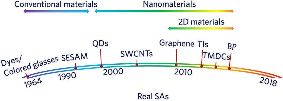
SAs in general can be broadly divided into two categories, namely real SAs, materials that exhibit an intrinsic decrease in absorption with increasing light intensity, and artificial SAs, devices that utilize nonlinear effects to imitate the action of a real SA by inducing an intensity-dependent transmission. In this article, we restrict the discussion to the nonlinear optical materials that are commonly used as real SAs. Thanks to the astonishing development in material science and microfabrication technology, an increasing number of novel material families have been employed as SA elements (Fig. 1). Sprouting from organic dyes and colored glasses, then flourishing and popularizing due to semiconductor materials [semiconductor SA mirrors (SESAMs) and carbon nanotubes (CNTs)], and nowadays further spreading to graphene and related two-dimensional (2D) layered materials, the SA element is becoming an indispensable component in modern ultrafast laser technology[10–13]. Furthermore, the increasing diversity of SA types provides more possibilities both in laser performance and integration designs. Conventional SAs are generally used in transmission and/or reflection via being inserted into laser cavities, while some newly developed nanomaterials can be integrated in a more compact way, for example, by transferring the SA materials onto the target gain media, such that the SA materials can interact with the laser modes directly or via the evanescent field[11]. The latter strategy allows for a monolithic solution when adopting waveguide technology. It is, hence, perceived to be a useful scheme to reach or at least to approach the ultimate level of on-chip integration in robust and compact packages.
Sign up for Chinese Optics Letters TOC. Get the latest issue of Chinese Optics Letters delivered right to you!Sign up now
Figure 1.Evolution of real saturable absorber (SA) technologies starting from conventional materials, such as organic dyes, colored glasses, chromium-doped crystals, and semiconductor SA mirrors (SESAMs), to nanomaterials, including zero-dimensional (0D) quantum dots (QDs), one-dimensional (1D) single-walled carbon nanotubes (SWCNTs), two-dimensional (2D) graphene, and graphene-like 2D layered materials, such as topological insulators (TIs), transition metal dichalcogenides (TMDCs), and black phosphorus (BP). Red dots denote the first, reported application of each technology in a pulsed laser.
Several reviews on solid-state waveguide lasers in general have been published[3,4,14,15]. Some further articles concentrate on more specific topics, for example, fabrication techniques[16–18], activators and gain media[19–22], and power scaling methods[23,24]. In this article, an overview of the progress to date in passive -switching and mode-locking of solid-state waveguide lasers is presented. Following the introduction, this article is structured as follows: firstly, we briefly discuss some critical points that are usually considered in the first place when designing a compact pulsed waveguide laser, including waveguide structure, SA-integration type, dispersion management, and cavity design; then, we overview the experimental results of mode-locked and -switched waveguide lasers. We also compare their laser performance according to fabrication techniques. Finally, a summary of this article and an outlook on future research in this area are given.
2. WAVEGUIDE LASER CAVITIES
A. Waveguide Structures
Common types of optical waveguides include optical fibers, rectangular and slab dielectric waveguides, and photonic crystal waveguides. This article concerns only optical waveguides defined in solid-state gain media by material deposition/bonding and modification techniques. Waveguide structures are generally classified into two typical configurations according to their geometries, namely slab-like guiding layers (planar waveguides) offer one-dimensional light-field confinement and tunnel-like guiding cores (channel waveguides) provide an additional dimension of confinement. Thanks to the diversity of fabrication techniques, waveguides with different geometries can be defined in various solid-state gain media. Planar waveguides in asymmetric slab [Fig. 2(a)] and symmetric slab/sandwich [Fig. 2(b)] types can be fabricated by employing surface-modification, layer-deposition, and wafer-bonding techniques. Channel waveguides in embedded [Fig. 2(c)], ridge [Fig. 2(d)], and buried [Fig. 2(e)] configurations can be defined based on the etching/ablation of planar waveguides and/or on localized-modification techniques[3].
Figure 2.Schematic diagrams of different types of planar and channel waveguides.
Optical waveguides are far more than merely connecting elements within integrated optical components and circuits. Benefiting from their strong optical confinement and miniaturized footprints, optical waveguides are fully capable of acting as functional active optical devices as well. Typical representatives are solid-state waveguide lasers, sources being of great potential for integrated optics because they are able to offer enhanced optical gain, reduced lasing threshold, and miniaturized footprints[4]. Generally, a good beam quality, e.g., diffraction-limited Gaussian beams with close to 1, is beneficial for efficient laser pulse generation, especially for mode-locked operation in waveguide lasers, since the excitation of higher-order transverse modes would disturb the pulse formation process via intermodal dispersion.
The number of the transverse optical modes at wavelength that a waveguide can support is given by[25]and for symmetric slab and buried channel waveguides, respectively. Here, and refer to the thickness of the slab waveguide and the width of the channel waveguide with a square-shaped cross section, respectively. The numerical aperture (NA) of a waveguide is defined as the sine of the maximum acceptance angle of an incident ray with respect to the waveguide axis. According to Eqs. (1) and (2), a single-transverse-mode waveguide can be achieved by properly designing its core size and refractive-index change. In this respect, the optimal fabrication technique/recipe with a view to achieving high-performance waveguides (low-loss and single-mode guidance) with small dimensions in a certain gain medium has to be identified.
B. Saturable Absorber
1. Numerical Analysis
An SA is an optical component that allows light to pass through if a certain intensity level is exceeded, or in another word, discriminates between low- and high-energy pulses[10]. In this way, when it is placed in a laser cavity, an SA will attenuate low-intensity continuous-wave (CW) light but release sufficiently high-intensity pulse spikes. Such phenomena can occur, theoretically, in any absorbing material in their corresponding resonance absorption wavelength ranges.
An ideal SA material is required to possess a strong intensity-dependent absorption, which can be described by a two-level model: where is the non-saturated but saturable loss coefficient, and is the saturation intensity of the SA. The coefficient also defines another key parameter of the SA, i.e., modulation depth[26]:
The modulation depth , the recovery time , and saturable intensity , are the core parameters of the SA. is the decay time for recovering the absorption of the SA after the emission of laser pulses, is the value of incident light intensity , for which the absorption falls to one-half of its initial value, and is the maximum change on the transmittance/reflectivity of the SA.
For a passively -switched solid-state waveguide laser operating well above threshold, the relevant quantities, namely, the pulse energy (), pulse duration (), and repetition rate (), could be, respectively, expressed as[26]where , the photon energy at the lasing wavelength, , the emission cross section of the laser material, , the mode size depending on the dimensions of the waveguide volume, , the cavity round-trip time determined by the cavity length , , the upper-state lifetime of the gain medium, and , the small-signal gain coefficient, which is also related to the pumping conditions, are the parameters of the solid-state gain medium. , the output coupling coefficient defined by the transmission of the output coupler, is the parameter of the laser mirrors in a waveguide laser system. , a parasitic loss coefficient that is usually dominated by the non-saturable loss of the SA, and the saturable loss coefficient are the parameters of the SA. Note that, for passive -switching operation, the time distance between two adjacent pulses is far longer than the SA recovery time or the pulse duration . Typical values of these three parameters in -switched solid-state waveguide lasers are of the order of picoseconds to nanoseconds for and , whereas microseconds for . Therefore, numerical analysis of SAs for the -switched operation could be conducted under the consideration of only fast SA models.
Equations (5)–(7) indicate that for a given solid-state gain medium and pumping conditions with fixed , , , and , high-energy and short laser pulses could be achieved not only from passively -switched waveguide lasers with large mode size and short cavity round-trip time , but also from the SA material with low non-saturable loss and, more importantly, high modulation depth (). It is clear to conclude that the modulation depth of an SA is a key factor that significantly impacts the -switched laser performance. It is also one of the most important indicators for characterizing and evaluating -switch elements.
Considering a passively mode-locked waveguide laser with an ideal SA, the shortest full-width at half-maximum (FWHM) duration of generated pulses could be expressed as[27]where is the gain and possible filter dispersion. This equation is only valid for pulse formation without group delay dispersion (GDD) and self-phase modulation (SPM). With this assumption, it is clear from Eq. (8) that SAs with large modulation depth would tend to favor the formation of ultrashort laser pulses.
In a more common case, negative GDD occurs in mode-locked solid-state lasers and results in soliton-like pulse shaping, which is the so-called soliton-mode-locking regime. This shaping process helps to compress the pulse shorter than the width of the net gain window. In fact, for fast SAs operating in this regime, the duration of the generated laser pulses is about two times shorter than that without soliton-like pulse shaping, which makes Eq. (8) be[27]
While in the slow SA case, the reduction in pulse duration can be even larger than a factor of two because the shaping process is reduced. The relation between pulse duration and pulse energy is[27]with in which the dispersion coefficient is a measure of the pulse-time broadening per unit distance per unit spectral width [s/(m·nm)]. is the SPM coefficient, which could be given by the nonlinear refractive index of the gain medium, the effective laser mode size , the length of the gain medium , and the lasing wavelength according to .
A passively mode-locked laser system could always generate shorter pulses by employing an SA element with larger modulation depth. However, the cost of this is the undesired non-saturable losses, which would increase with high modulation depth and could reduce the laser performance or even cease the laser emission. Therefore, a given SA with certain modulation depth should be utilized as efficiently as possible for the generation of the shortest pulses. A very interesting phenomenon is that almost equally short pulses could be obtained from passively mode-locked lasers when using fast and slow SAs with the same modulation depth. This could be attributed to the higher saturation level the slow SA owns when the response time is much longer than the pulse duration. However, pulses produced by employing the fast SA are superior in terms of pulse quality and stability[27].
2. Integration
For real SAs, two subcategories can be distinguished on the basis of materials families: conventional materials, such as organic dyes, ion-doped crystals, SESAMs, and nanomaterials, including CNTs, graphene, and graphene-like 2D layered materials[12]. According to the applied absorbing materials, SAs can be incorporated into waveguide laser cavities in different manners, including direct-interaction-type SAs, such as SA glasses/crystals used in transmission and SA mirrors operated in reflection, and evanescent-field-interaction-type SA thin films (Fig. 3).
Figure 3.Common strategies of transferring SA materials on optical substrates on (a) transmitting glass plates, (b) reflecting mirrors, and directly on (c) exposed waveguide surfaces.
Transparent ion-doped crystals, e.g., chromium ()-doped crystals, can be directly incorporated into the laser cavity as free-space SA elements. Some other materials, e.g., organic dyes and nanomaterials, can be firstly deposited/spin-coated on transparent glass/crystal plates or on cavity mirrors and then used in transmission/reflection. In a more compact configuration, the absorbing material can be directly transferred onto the end-facet of the waveguide, serving as an outcoupling mirror in parallel. If the waveguide gain medium exhibits high gain and low loss, only the Fresnel reflections at the incoupling and outcoupling end-facets can provide sufficient optical feedback for laser oscillation. In such an SA-alignment-free scheme, a monolithic laser cavity that is more stable and invulnerable to external disturbances can be realized. For example, in a recent work, monolayer graphene films prepared by chemical vapor deposition (CVD) on copper foil are subsequently transferred onto the outcoupling mirror and the waveguide end-facet. In both cases, comparable -switched waveguide laser performance is achieved[28], suggesting great potential of such a compact configuration for developing monolithic laser devices.
In a very compact scheme, the SA material that is coated on top of an active waveguide core can also interact with the laser modes via the evanescent field. Practically, this method is usually realized by transferring the SA material onto the top surface of the target waveguide using polymer composites as supporting layers. Such an SA-integration technique was firstly demonstrated in fiber lasers[29], and it has been also deployed for -switching of waveguide lasers in a number of solid-state gain media since 2008[30].
Most compact pulsed lasers are operating in the self-pulsed regime without any additional SAs. Some Cr-doped laser crystals, such as neodymium () and co-doped yttrium aluminum garnet (YAG), gadolinium vanadate (), and yttrium orthovanadate () crystals, are able to realize self--switched operation. Particularly, a self--switched channel waveguide laser has already been realized[31]. The optical feedback therein is given only by the Fresnel reflections at waveguide end-facets, demonstrating a truly monolithic laser cavity. Alternatives for realizing self--switched pulsed lasers are composite gain media, for example, diffusion-bonded Nd:YAG/Cr:YAG crystals. These crystals are reported to be able to generate pulses with up to 4 kW peak power based on channel waveguide geometries[32,33].
C. Pulsed Waveguide Laser Cavities
With the employment of either transmission- or reflection-type SA elements, pulsed waveguide lasers based on a direct-field-interaction scheme can be constructed, as sketched in Fig. 4(a). Interaction occurs in this scheme when the central peak of the propagating optical mode passes through the nonlinear material. This scheme offers a few distinct advantages, e.g., simplicity in preparation process, broad compatibility with various waveguide configurations, and full optical power involvement in the interaction. The direct-interaction method is the most commonly used scheme for passively mode-locking and -switching of waveguide lasers, and it has been applied for almost all types of waveguide geometries. Since the SA element employed in this configuration usually acts also as an outcoupling mirror, it is therefore very convenient to tune the distance between the SA and the waveguide end-facet, offering a short laser cavity with flexible length for efficient dispersion management and stability enhancement[34–41]. Detailed discussion concerning this effect can be found in the next section.
Figure 4.Schematic diagrams of two typical end-pumping configurations of passively -switched and mode-locked waveguide lasers based on (a) direct-interaction and (b) evanescent-field-interaction schemes.
In contrast to the direct-field interaction, evanescent-field interaction [Fig. 4(b)] involves only a portion of the intracavity optical power, thus naturally increasing the laser damage threshold of the SA. Furthermore, the increase in interaction length (by several to tens of orders of magnitudes) not only enhances the overall nonlinear interaction, but also allows for simpler SA transfer, easier alignment to the guiding core, and less sensitive operation conditions compared to the direct-interaction scheme, thus resulting in less complicated mode-locked and -switched operation. Since the SA in the evanescent-field-interaction scheme is not in the path of the laser beam, optical and mechanical damages to the SA are much less critical. However, the SA used in this scheme has to be coated on the exposed guiding core instead of the end-face in order to interact with the evanescent field of the optical modes. This is unfortunately only possible so far for waveguide structures with superficial types, e.g., asymmetrical slab [Fig. 2(a)], embedded [Fig. 2(c)], and ridge waveguides [Fig. 2(d)]. Up to now, stable mode-locking of the waveguide laser under this scheme, however, is not yet demonstrated due to the insufficient and incomplete interaction between the guided light field and SA when using relatively short waveguide cavities.
This review article mainly concerns compact monolithic and quasi-monolithic cavities. What is noteworthy is that, in the monolithic cavity, it is however difficult to find the correct SA properties, while in an extended cavity one can easily shape the beam so that the intensity on the SA is good for the desired operation mode. Besides, dispersion control is much simpler in the extended cavity scheme, as discussed in the following section.
D. Dispersion Management
Two of the most critical factors regarding achieving a CW mode-locked waveguide laser are to significantly reduce the level of waveguide loss and to effectively control the material dispersion in the laser system. Waveguide loss originating from scattering, material absorption, radiation, and optical coupling can be efficiently suppressed via perfecting the waveguide structure design and optimizing the fabrication technique. One can refer to Ref. [3] for detailed analyses concerning the waveguide loss mechanisms and measurement methods. Here, we only focus our discussion on the dispersion management in a waveguide cavity.
In a compact waveguide laser cavity, the naturally occurring chromatic dispersion introduced by the gain medium is often in the normal regime. The desired net cavity dispersion may either be close to zero or even anomalous (for soliton formation mechanism). Typically, such dispersion values can be achieved by introducing optical components, e.g., dielectric dispersive mirrors, prism pairs, and diffraction gratings, with anomalous dispersion into the laser cavity[42]. To this end, the external cavity scheme that contains waveguide and free-space or fiber-based optical propagation is commonly used, as sketched in Fig. 5(a). In this way, however, the cavity will be greatly extended. To realize efficient mode-locking and in parallel to maintain the cavity compactness as much as possible, researchers utilized a thin air-filled gap between the waveguide’s end-facet and a cavity mirror or an SA element, as sketched in Fig. 5(b), for interferometric dispersion control[34–40]. This air-filled gap can be considered as an equivalent Gires–Tournois interferometer (GTI)/etalon structure, which is capable of fully balancing the GDD and the SPM of the waveguide cavity to avoid the formation of chirped pulses. The dependence of the GDD introduced by the GTI on the air-filled gap size and the lasing wavelength is expressed by the following equation[43]: where is the angular frequency of the laser, is the reflectivity of the waveguide, and is the round-trip time for the light in the GTI gap. An example illustrating this dependency can be found in Ref. [40]. Moreover, this strategy is also beneficial for stabilizing -switched lasers in a high-power-pumping operation via preventing excessive loss due to diffraction in free space[41]. However, with such an air-filled gap, the waveguide cavity is intrinsically not fully monolithic.
Figure 5.Schematic diagrams of two commonly used strategies for dispersion management in mode-locked waveguide lasers based, respectively, on (a) extended cavities and (b) soliton formation mechanisms realized by adjusting the cavity length, i.e., by tuning the air-filled gap between the SA and waveguide end-facet.
Generally speaking, it is very difficult to obtain a satisfying dispersion control inside a compact waveguide cavity. One possible solution is a multi-functional mirror, which acts at the same time as an incoupling/outcoupling mirror and as a dispersive GTI mirror. It should, however, be noted that it is very difficult to precisely control the dispersion of a GTI mirror in the regions of a steep change of the reflectivity that are necessary for providing desired optical feedback. Moreover, for such a mirror to work in a fully monolithic setup, the coating needs to be designed, considering that the mirror interface is to waveguide material instead of air. Such a mirror could even be coated directly onto the end-facet of the waveguide, but this requires a precise knowledge of the waveguide dispersion at the targeted optical power level. If these challenging requirements can be fulfilled, a fully monolithic mode-locked waveguide laser with near-Fourier-limited pulse duration is within reach.
3. DEMONSTRATION AND DISCUSSION
Fabrication of highly efficient and practical waveguide lasers in a variety of solid-state gain media is in any case the primary task to be performed. The key point is to construct a higher index core, i.e., waveguide core, surrounded by lower index layers, which can be air and/or cladding. There are a number of fabrication techniques that have been employed for constructing solid-state waveguide lasers, which in general can be subcategorized into two fundamental categories: one can be described as the formation of an active material film grown/bonded onto the top surface of a lower index substrate, forming a step-index waveguide, and the other one relies on an introduced graded-index modification inside an existing bulk material via surface microstructuring or subsurface localized micromachining techniques[3]. In this section, we discuss and compare the performance of pulsed waveguide lasers fabricated by different techniques.
A. Figure of Merit
To provide an intuitive view of the laser performance and a quantitative comparison of the experimental results, here we define a figure of merit (FOM) given by the product of the pump-to-peak-power enhancement factor and the maximum quantum-defect-limited efficiency, namely, where the maximum peak power value at laser wavelength is calculated based on the duration , the repetition rate , and the maximum average power of the output laser pulses. denotes the absorbed pump power at pump wavelength .
To get a rough idea of the FOM value for a pulsed waveguide laser, let us assume the output laser beam has an ideal Gaussian intensity profile, and the laser efficiency is only limited by the quantum defect. If the lasing threshold is far lower than , the product of and is close to 1. In case of the mode-locked laser, is a fixed value determined by the length of the waveguide cavity. Then, the FOM value is mainly determined by the last factor . According to the Fourier transform, the lowest is limited by the minimum possible time-bandwidth product , which is for Gaussian-shaped pulses, i.e., bandwidth-limited pulses. This gives us an upper limit of the FOM value for a mode-locked waveguide laser in the gain medium with a gain bandwidth (in frequency space) of . Apparently, higher and lower slope efficiency, which are caused in most cases by high waveguide loss and/or low gain efficiency of the gain medium, would make the product of and lower than 1, reducing the FOM value.
Figs. 6(a)–6(c) present the FOMs of solid-state waveguide lasers operating in the passively -switched [Figs. 6(a) and 6(b)], -switched mode-locked [Figs. 6(a) and 6(b)], and mode-locked [Fig. 6(c)] regimes versus the waveguide footprint/volume defined by different fabrication techniques. The footprint/volume values are given by the products of the waveguide thicknesses and lengths for planar waveguides and by the products of the waveguide cross-sectional areas and lengths in case of channel waveguides, respectively. It is worth noting that the data points (with approximately 10% errors) shown in Figs. 6(a)–6(c) leave some factors out of consideration, such as pump sources (diffraction-limited lasers or diode bars/stacks), SA materials, and host gain media, some of which are involved in the following discussion. Besides, the FOM calculation used here is fair for evaluating laser performance of different waveguides in the same operation regime. But, one should not compare directly, for example, the FOM value of a -switched waveguide laser to that of a CW mode-locked one, because in most cases the latter one exhibits much better waveguide quality, cavity dispersion control, and laser performance even with a lower FOM.
Figure 6.Figures of merit (FOMs) of pulsed waveguide lasers operating in the -switched and -switched mode-locked regimes with (a) planar and (b) channel geometries, as well as in (c) the CW mode-locked regime. The FOM errors in these diagrams are . The symbols’ colors represent waveguide fabrication methods, while the symbols’ appearance stand for different laser configurations in terms of operation regimes, waveguide geometries (circles, -switched; triangles, -switched mode-locked; squares, planar waveguide lasers operating in the CW mode-locked regime; stars, channel waveguide lasers operating in the CW mode-locked regime) and SA integration types (open markers, free-standing SAs inserted in cavities; filled markers, integrated SAs coated on waveguides).
1. Pulsed Laser Deposition of Slab Waveguide Lasers
Pulsed laser deposition (PLD) is a simple and versatile technique for fabricating multi-functional thin film devices, including planar waveguide lasers in well-established materials, such as RE-doped garnets and titanium-doped sapphire (Ti:sapphire), as well as in emerging materials like RE-doped sesquioxides and Nd:sapphire[44–51]. In a typical PLD workstation, as sketched in Fig. 7(a), a high-power pulsed laser beam (generally with laser fluence of ) focused on the target is used to vaporize a small amount of material, ejecting a bubble of hot laser plasma plume that contains gaseous particles from the target surface. Shortly after it impinges on the substrate surface, particles in the plasma interact with each other and also with the substrate and start to nucleate. In this way, the evaporated plume may condense on the substrate surface, eventually forming stoichiometric thin film growth.
Demonstration of PLD-grown pulsed waveguide lasers is so far limited to only ytterbium-doped yttria ()[48,49], a typical representative of sesquioxide crystals offering an even higher thermal conductivity than that of YAG. In two correlated studies from the same research group, -switched operation of planar waveguide lasers using graphene SAs is reported, providing pulses with 98 ns in duration and average output powers up to 456 mW[48,49]. Both works use YAG as deposition substrates for epitaxial growth of layers, as illustrated in Fig. 7(b), forming asymmetric slab geometries with 6- and μ-thick guiding cores. The graphene films are coated on the outcoupling mirror[48] and on the waveguide top surface[49], serving as SAs through direct- and evanescence-field-interaction processes. By comparison, the pulse energy produced in the evanescence-field-interaction case is higher, reaching 310 nJ with the pumping of high-power broad-area diode lasers. However, the laser performance in both studies still suffers strongly from the relatively high scattering losses, resulting in non-uniform mode distributions [as shown in Fig. 7(c)] and unwanted thermal effects[51], as also implied by their FOMs in Fig. 6(a). Partly due to the high losses, there are still no reports on PLD-grown channel waveguide lasers operating in the pulsed regime.
The relatively high losses of PLD-grown waveguides are mainly originated from the micron-sized particulates that are present on the film surface and embedded in the guiding layer. This “large particulate” problem is actually one major intrinsic drawback of the PLD-grown films and can hardly be avoided by merely optimizing experimental parameters or be completely removed by subsequent fine polishing processes. For materials with anisotropic crystalline properties, this problem can even be particularly severe[44]. Some approaches that have been proved effective to reduce the average size and quantity of the particulates and hence decrease the waveguide losses are realized by using, for example, picosecond and femtosecond (fs) pulsed lasers for target ablation, synchronized pulsed gas-jet configuration, collision of crossed plumes, spinning high-density targets, modified off-axis deposition geometry, and vane velocity filters[44].
Even though with the intractable particulate issue, PLD is still a functional technique because it is capable of near-perfectly replicating the composition of the target material in the deposited film without contaminant. This feature can be particularly beneficial for the growth of, for example, sophisticated films with mixed materials, multi-element doping, and multi-layer structures by using multi-target, multi-beam setups[44,45], for example, the dual-target and dual-beam setup, as shown in Fig. 7(a).
2. Liquid Phase Epitaxial Growth of Slab Waveguide Lasers
Liquid phase epitaxy (LPE) is a technique by which a dielectric planar waveguide layer, generally with an asymmetric slab geometry, can be grown from a dilute molten solution on a flat oriented single crystal substrate[20,52], as sketched in Fig. 8(a). The LPE layer growth process is isothermal, which can ensure homogeneous composition across the whole core layer, allowing the growth of high-quality waveguides with extremely low propagation losses[53].
One main branch of LPE-grown pulsed waveguide laser research in recent years is RE-doped, particularly Yb- and thulium (Tm)-doped, potassium yttrium tungstates [ or KYW]. Monoclinic potassium double tungstates are extremely promising for laser research because they can be heavily doped with RE ions. For example, the -doping concentration can be even comparable to stoichiometric structure [20]. Through direct- and evanescence-field-interaction processes, LPE-grown Yb:KYW/KYW planar waveguide lasers operating in the -switched regime using SESAM[54], single-walled CNTs (SWCNTs)[55], and graphene[56] SAs have been demonstrated, delivering pulses with durations as short as 170 ns and repetition rates as high as 722 kHz. In addition to -doping, KYW crystals also have advantages of efficient, low-threshold -doped laser operation in terms of, for example, high absorption and emission cross sections. So far, pulsed laser emission in the μ spectral range has been demonstrated in LPE-grown Tm:KYW/KYW planar waveguides [Figs. 8(b) and 8(c)][57–59]. In these studies, Ti:sapphire lasers operating at 802 nm are used as pump sources. -switched laser pulses with a duration as short as 83 ns and energy up to 120 nJ have been produced using -doped zinc selenide (Cr:ZnSe)[57], graphene[58], and SWCNT[59] SAs via direct-field interaction. One common shortcoming of these studies lies in the relatively low laser slope efficiency (average output power), which is so far limited to 20% (50 mW). This is partly due to the multi-transverse-mode operation, giving relatively low FOMs, as shown in Fig. 6(a). Further power scaling and shortening of the laser pulses are expected by optimizing optically active, i.e., , and inert, e.g., lutetium () and gadolinium (), ion concentrations and, remarkably, by substituting the planar structure by channel geometry. In the latter case, CW laser slope efficiency close to quantum-defect-limited values is achievable[60,61]. Besides, single-transverse-mode operation with better beam quality is readily accessible with channel waveguides.
3. Summary
There is still much room for improving the laser performance of epitaxially grown waveguides with a view to achieving higher pulse energy via -switched operation and realizing the very first demonstration of stable mode-locked operation. To this end, apart from constantly optimizing the growth recipes, some promising gain media, such as PLD-grown RE-doped garnet and LPE-grown RE-doped yttrium lithium fluoride (YLF) waveguide lasers, can be considered[46,62,63].
C. Wafer Bonding of Waveguides
1. Contact Bonding of Slab Waveguide Lasers
Contact bonding is a phenomenon that optically polished, flat, and clean wafers, when brought into contact, bond to each other without using adhesives or external forces, solely as a result of long-range van der Waal’s attractive intermolecular forces. Contact-bonded waveguides generally possess extremely low scattering losses as a result of atomically smooth interfaces. Furthermore, this fabrication technique is capable of breaking through the constraints imposed on the selection of substrates for epitaxially grown waveguide layers and, in parallel, offering considerably large refractive-index differences between the guiding core and the cladding. The generally large NAs of contact-bonded waveguides happen to be well-suited for diode-laser-pumping configurations[23,24]. In addition, the double-clad waveguide design (symmetric slab geometry), which is readily accessible with contact bonding, provides an efficient way to achieve good power scalability and, in parallel, to maintain a good spatial mode quality in the guided dimension under high-power-pumping operation[23,24].
RE:YAG crystals with outstanding laser and thermo-mechanical properties are in most cases the first choice for constructing diode-pumped contact-bonded waveguide lasers[64–67]. By replacing a section of the guiding layer (in double-clad Nd:YAG and Yb:YAG planar waveguides with symmetric geometries) in the core with a passive -switch, μ laser pulses with 3 and 1.6 ns in duration at repetition rates of 80 and 76 kHz are delivered, respectively[64,65]. These results correspond to high peak powers of 28 and 18 kW, representing the highest values for pulsed planar waveguide lasers, as indicated in Fig. 6(a). Furthermore, based on the end-pumping configuration, single-mode operation with good output beam quality ( values of ) is achieved in spite of using broad-stripe laser diodes as pump sources[65]. To further improve the beam quality, one can consider channel geometries, as depicted in Fig. 9, which are able to not only produce CW output with laser efficiencies near to quantum-defect-limited values, but also generate nearly diffraction-limited Gaussian beams with [67]. More recently, this strategy is adopted in the very first demonstration of holmium ()-doped YAG channel waveguide lasers operating at μ[66]. The waveguide structure is prepared via bonding of a Ho:YAG core to an undoped YAG cladding. Laser pulses with an energy of up to μ at a repetition frequency of 442 kHz are achieved by employing a switch.
Figure 9.(a) Optical microscope image of the end-facet of the Ho:YAG channel waveguide fabricated by direct bonding. (b) Photograph of the Ho:YAG waveguide sample. (c) Measured modal profile of the Ho:YAG channel waveguide laser. Reproduced with permission from Ref. [66].
One main shortcoming of bonded sandwich-like waveguides is their large footprints. This point cannot be directly reflected from Fig. 6(a), because the calculation there considers only the sizes of the waveguide cores. The additional footprints are introduced by the double-clad structures, which generally consist of an active waveguide core layer and four-layer claddings made of YAG (inner claddings) and sapphire (outer claddings)[64,65]. Besides, multiple optically precise lapping/polishing and crystal-bonding processes are needed for achieving channel waveguide cores with the desired dimensions, for example, the waveguide structure in Ref. [66].
2. Tape Casting of Slab Waveguide Lasers
Recently, an established ceramic fabrication technology, namely the tape-casting method, was introduced to fabricate ceramic sandwich-like waveguide lasers[68–70]. In this process, three-segment-composite structures [symmetric slab configuration, as sketched in Fig. 10(a)] are fabricated based on the solid-state reactive sintering approach, converting ceramic powder into thin films[68]. Apparently, this technique specializes only on ceramic waveguide lasers and thus, to a certain extent, lacks applicability to a wide range of materials. A unique advantage that distinguishes tape casting from other waveguide fabrication methods is that this technique is able to offer a simple way to form a monolithic structure that is composed of multiple layers with different base compositions and variable thicknesses[68].
Figure 10.(a) Schematic diagram of the YAG/RE:YAG/YAG planar waveguide fabricated by tape casting. (b) Measured modal profile of the SESAM mode-locked YAG/Yb:YAG/YAG waveguide laser. Reproduced with permission from Ref. [69].
The footprints of tape-cast waveguide lasers are so far within the largest scale for any type of planar waveguide laser. The standard core thickness is around 0.1 mm. This perhaps explains why this is one of the limited techniques that have been proven useful for realizing CW mode-locked planar waveguide lasers, as indicated in Fig. 6(c). By employing tape-cast YAG/Yb:YAG/YAG planar waveguides and SESAM, researchers achieve 2.95 ps laser pulses with average output powers up to 385 mW in the CW mode-locked operation[69]. The output beam has values of 1.1 and 1.42 in the unguided and guided directions, respectively, as shown in Fig. 10(b). Besides the large footprint, one shortcoming of this laser is that the waveguide therein is placed inside a -shaped laser cavity, extending the overall cavity length to over 1 m[69]. In a separate study employing a short waveguide cavity, a -switched laser with a pulse duration of 179 ns and a pulse energy of 221 nJ is realized[70].
3. Summary
Wafer-bonded planar waveguides are inherently compatible with high-power diode-pumping configurations because, first, their planar geometries match well to the diode laser beam profiles; second, their accessible large NAs offer efficient pump launching even using highly divergent pump beams. As a fundamental requirement for power scaling, gain media have to possess good thermal properties. This is the main reason why most of the reports of such devices are implemented based on RE:YAG. Future works within this topic may focus on reducing the overall single-/double-clad waveguide dimensions without weakening their capabilities of power scaling and spatial mode control.
D. Surface Modification of Waveguides
1. Ion Implantation/Irradiation of Surface Waveguide Lasers
Waveguide definition through ion implantation essentially depends on the material modification introduced by accelerated high-energy positive ions bombarding the target[17]. During this process, incoming charged ions gradually lose their energy while interacting with nuclei and electrons of the target material and eventually get stopped in the near-surface region several micrometers beneath the surface. As a result, one could achieve the desired refractive-index change for surface/near-surface waveguide layer formation in the irradiated region. Up to now, optical waveguides have been successfully fabricated by ion implantation in a variety of optical materials, including inorganic and organic materials[17]. Unlike epitaxial growth and bonding techniques, patterned geometries can be easily introduced in ion-implanted waveguides by masking the substrates. This allows for flexibly designed waveguide geometries (embedded geometries) without using any post-structuring techniques, as shown in Fig. 11.
According to the applied ion species and ion energy, ion implantation/irradiation can be subcategorized into three groups, namely light-ion implantation, heavy-ion irradiation, and swift heavy-ion irradiation. Material modification mechanisms for these schemes are different, resulting in different refractive-index profiles in waveguides[17]. This provides a large degree of freedom for the waveguide design. However, the common shortcoming of both light- and heavy-ion-implantation/irradiation waveguides is the increase of optical scattering losses caused by lattice distortions and defects created inside guiding cores and/or at guiding boundaries. This side effect, in most cases, can be effectively eased by thermal annealing treatment[17].
Waveguide lasers fabricated by ion implantation/irradiation have been successfully realized in a wide range of laser crystals. The applied ion species encompass protons, hydrogen (), helium (), carbon (), nitrogen (), oxygen (), silicon (), argon (), and krypton ()[17,71–79]. The first -switched ion-implanted waveguide laser is demonstrated in a Si-ion-implanted waveguide cavity using a gallium arsenide (GaAs) switch, producing 3.88 ns pulses with peak power as high as 212 W[71], which corresponds to one of the largest FOMs in Fig. 6(a). Most of the following publications on this research topic since then are accomplished using Nd:YAG as gain media[72–79]. In these correlated studies, researchers from the same group use graphene[72–74,78] and graphene-like 2D nanomaterials, including TIs[75], TMDCs[76] and BP[76], as newly developed SAs in -switched operation. Through a direct-interaction process, laser pulses with repetition rates of 2–6 MHz and duration as low as 24 ns are achieved. In a more recent study, thermal tunability of the saturable absorption feature is evidenced in vanadium dioxide ()-based pulsed waveguide lasers[77]. As a result, the first picosecond (700 ps) waveguide laser is obtained by using a switch at its phase-transition point, giving relatively high FOM values, as shown in Fig. 6(a). In the evanescence-field-interaction case, laser performance is characterized with higher pulse energy but larger pulse widths[73], resulting in a comparable FOM to the direct-field-interaction processes. Most recently, the first demonstration of passively -switched waveguide lasers in disordered crystals is reported. A tungsten disulfide () film layer coated on the surface of a ridge Yb-doped yttrium scandium gallium garnet (Yb:YSGG) waveguide interacts with the evanescent field of the guided mode, producing 125 ns laser pulses at a repetition rate of 360 kHz[79].
More recently, ion implantation/irradiation is proved to be an effective approach to tailor the saturable absorption properties of SAs[80–85]. The irradiation-induced atom displacement/rearrangement in the target SA materials, for example, in graphene and thin films, is regarded as the main origin of the morphological change (topographic smoothing and layer space thinning) and the enhanced nonlinear absorption[81,82]. This strategy has been applied for -switching of waveguide lasers at the μ spectral band[81,82]. Alternatively, with the assist of post-annealing treatment, ion implantation/irradiation can be employed for synthesizing of embedded metal nanoparticles in crystals (Fig. 12), which show localized surface plasmon resonance (SPR)-induced nonlinear absorption enhancement over a broad spectral band[83–85]. For example, being embedded with plasmonic gold (Au) nanoparticles, Nd:YAG and lithium niobate () crystal wafers are able to passively switch and mode lock visible and near-infrared (IR) waveguide lasers, respectively[83–85]. These strategies provide novel concepts with a view to achieving more compact pulsed waveguide laser cavities and developing intriguing integrated photonic devices.
Ion exchange is a comparatively mature technique widely used for waveguide fabrication in glasses[86]. The concept of “exchange” herein means that the diffusant ions from certain melt sources immigrate to glass substrates and substitute relatively mobile ions, typically monovalent, e.g., sodium () and potassium (), which are originally in the glasses. Subsequently, native ions in glasses with smaller size and/or polarizability will be expelled into the melt, completing the “exchange” process. As a result, the desired refractive-index modification in selected sections of the host substrate could be achieved, forming surface waveguide structures with asymmetric slab geometries. Through a patterned mask, ion exchange can be used to fabricate embedded waveguides, as sketched in Fig. 13(a). By employing the electric field, particularly, ion migration from a molten salt at the anode side into the substrate, can be deepened, making the fabrication of buried waveguides even possible[86]. One challenge of the ion exchange technique is the insufficient controllability of the waveguide thickness and refractive-index profile, which needs thoughtful adjustment of the technology procedure. Besides, ion exchange is only valid for waveguide fabrication in glasses and in a limited number of crystalline materials, e.g., . Nevertheless, this technology enables low-cost and high-quality waveguides with fully reproducible properties once the fabrication recipe is well-adjusted.
RE-doped waveguide pulsed lasers fabricated by ion exchange have been reported in a number of glasses, for example, the pioneer demonstration of pulsed solid-state waveguide laser in Nd-doped phosphate glass[9]. The -switched laser described therein uses a bis(4-dimethylaminodithiobenzil)nickel (BDN) organic dye sheet as SA element, delivering 25 ns pulses with a peak power of 3 W[9]. The volume of the embedded waveguide used therein is one of the smallest among all the demonstrated pulsed waveguide lasers with channel geometries, as indicated in Fig. 6(b). In addition, the first studies of passively CW mode-locked waveguide lasers are carried out as well based on the ion-exchanged technique in erbium/ytterbium (Er/Yb) co-doped phosphate glass planar waveguides[87–89]. Based on the modulation of SESAMs, laser pulses with a duration of 1 ps and an ultralow timing jitter of 14.4 fs are achieved by using, respectively, an intracavity spectral filtering element[87] and a high-speed feedback control system[89]. These studies are really impressive in terms of laser performance, as suggested by their large FOMs in Fig. 6(c). However, they are benefiting from extended laser cavities.
The following research activities focus more on compact channel waveguide cavities[34–36]. By employing SESAMs as SAs, self-starting CW mode-locked lasers at 1 and μ are realized in Yb-doped and Er/Yb co-doped phosphate glass waveguides, generating laser pulses with repetition rates of 15.2 and 6.8 GHz, respectively[34–36]. The soliton formation mechanism is considered to be the cause of the stable mode-locked operation and sub-picosecond pulse (pulse durations as short as 0.7 and 2.5 ps for 1 and μ lasers) generation. The required negative dispersion therein is introduced into the laser cavity by controlling the air-filled gap between SESAM and the waveguide end-facet via the GTI effect. The excellent laser performance of these waveguides is also reflected by the single-mode operation with nearly diffraction-limited output ( values of ), as shown in Fig. 13(b)[35]. In a later study from the same group, -switched mode-locking and -switching of the same glass waveguides are realized using graphene SAs[90].
In a separate research branch, the pioneer studies on evanescent-field-interaction-based -switched waveguide lasers are conducted in Nd-doped phosphate glasses[30,91,92]. In these studies researchers use cellulose acetate polymer films doped with BDN dye as SAs, which are hybrized on waveguide surfaces. These devices are able to emit pulses with 1.3 ns width and 1 kW peak power[91]. The latter value represents one of the highest peak power values produced by -switched channel waveguides, as implied by the FOM values in Fig. 6(b). By utilizing an analogy configuration, in a later work, narrow-linewidth (372 MHz) -switched distributed Bragg grating (DBR) waveguide lasers are realized in Yb-doped alumino-phosphate glasses[92].
3. Summary
Surface-type waveguides fabricated by material-modification techniques, such as ion implantation/irradiation and ion exchange, have significant advantages over epitaxially grown and bonded waveguides in terms of geometrical flexibility. Particularly, a more flexible ion-beam-modification technique, namely focused ion-beam writing[93], has not yet been used for fabricating pulsed waveguide lasers. However, one main limitation for material-modification techniques, e.g., ion implantation/irradiation, with a view to achieving high-performance waveguide lasers is the lattice distortions and defects introduced by electronic and nuclear damages, resulting in high waveguide loss. Ion exchange has been proven to be a very useful and mature fabrication technique as implied by a number of milestones in waveguide laser research activities, including the first Q-switched waveguide laser[9], the first CW mode-locked waveguide laser[87], the first evanescent-field-interaction-based pulsed waveguide laser[30], and the first CW mode-locked waveguide laser with short cavity[34]. However, ion exchange is only useful for glasses and some crystals with chemically mobile elements. In contrast to ion exchange, the first CW mode-locked waveguide laser fabricated by ion implantation is not yet demonstrated. Further optimizing the optical setups by introducing better dispersion management, e.g., in analogy to that in Fig. 5(b), can be a useful strategy.
E. Localized Modification of Waveguides
1. Femtosecond Laser Writing of Channel Waveguide Lasers
In contrast to planar geometries, waveguide lasers in channel geometries provide noticeable advantages in terms of compactness, miniaturization, flexibility, and integration. Furthermore, it is much simpler in channel waveguides to maintain/achieve single-transverse-mode operation because of the better geometric symmetry. This may explain why fs-laser micromachining, as a “newly” discovered three-dimensional (3D) microfabrication technique, immediately delivered a stunning performance in designing compact waveguides in transparent dielectrics since the pioneer work in 1996[18,94–99].
Tightly focused fs-laser pulses are able to modify the optical properties of a small volume inside a transparent substrate. Based on this, a localized and designable refractive index modification can be introduced in a direct procedure without using patterned masking, allowing waveguide (generally with buried geometries) fabrication in an extremely flexible way by simply scanning the laser beam or the target substrate. This technique is applicable to a large number of optical materials. Detailed discussion on the material-modification mechanism of fs-laser micromachining can be found in Refs. [18,96].
Generally, the identified structural modifications in transparent dielectrics induced by fs-lasers can be mainly subcategorized into two types, depending on whether the working intensity of the fs-laser pulse exceeds the optical damage threshold of the irradiated dielectrics or not. In case of low-intensity laser irradiation, i.e., the so-called weak damage regime (Type-I modification) working below the optical damage threshold, a smooth refractive-index change at the focal volume is formed. In contrast, for high peak intensities, severe damage (Type-II modification) with localized defect formation and material network rearrangement is generated[18,99,100]. The sign of the refractive-index change strongly depends on the modification mechanisms, or more fundamentally, on the laser exposure conditions and target materials. Usually, the most commonly used morphological geometries of waveguides in transparent dielectrics are characterized as tunnel-like “single-line” (Type-I modification), stress-field-induced “double-line” (Type-II modification), and fiber-like depressed-cladding (Type-I or Type-II modification) waveguide structures, as illustrated in Fig. 14. So far, waveguide lasers based on different geometries defined by fs-laser writing have been realized in various solid-state gain media, spanning from single crystals and polycrystalline ceramics to amorphous glasses[18,99].
Studies on SA-based fs-laser-inscribed pulsed waveguide lasers start from CW mode-locked operation in single-line waveguide lasers in Er/Yb co-doped phosphate glass and Er-doped bismuthate glass substrates[101,102]. By employing extended fiber ring cavities and inserting specially designed fiber-pigtailed SWCNT polymer films into the cavities, 320 fs pulses with a repetition rate of 40 MHz at μ are produced[102]. In order to improve the compactness of the laser cavity, a following study uses a two-mirror waveguide cavity[103]. However, due to the lack of dispersion management, researchers only achieve -switched mode-locked operation, producing 1.06 ps pulses with a repetition rate of 1.5 GHz at 1039 nm from single-line waveguides in Yb-doped bismuthate glasses[103]. A graphene-coated outcoupling mirror is used as an SA therein. Based on the analogy cavity configuration in the following studies, 7.8, 5.9, and 6.5 GHz laser pulses are obtained from Tm:YAG, Ho:YAG, and cladding waveguides in -switched mode-locked operation[84,85,104–106]. In contrast, by employing extended cavities, the common repetition rate of -switched mode-locked laser pulses achieved is [107,108]. These results clearly reflect the typical features of pulsed laser performance given by a compact waveguide cavity: high repetition rate but difficult dispersion management. The successful demonstration of CW mode-locked operation in fs-laser-written waveguide lasers is inspired by the abovementioned ion-exchanged waveguide lasers (discussion in Section 3.D.2.), in which an adjustable air-filled gap is introduced into the cavity to control the dispersion via the GTI effect. Consequently, stable CW mode-locking of Nd:YAG cladding and Yb:YAG double-line waveguides is realized, generating pulses with durations of 16.7 and 1.89 ps, as well as repetition rates of 11.3 and 2.08 GHz, respectively[37–39]. Most recently, fs-laser pulses have been achieved from Ti:sapphire double-line waveguide lasers[40]. The time duration of 41.4 fs and the repetition rate of 21.25 GHz therein both represent the record short/fast values for any type of CW mode-locked waveguide lasers so far, which is benefiting from the precise tailoring of the GDD by means of the GTI effect, as well as the broad gain bandwidth of Ti:sapphire[40]. In a separate work, by using an Er/Yb/Ce co-doped ZBLAN glass (fluorozirconate glass with the composition ) cladding waveguide with an extended laser cavity, mode-locked laser pulses with a duration of 180 fs and a repetition rate of 156 MHz are produced[109]. The spectral bandwidth of the 1550 nm output therein is 25 nm, which is the first experimental evidence to support more than 10 nm spectral bandwidth in a passively CW mode-locked waveguide laser. There are also examples of effective CW mode-locked operation in waveguide lasers without any dispersion compensation, as demonstrated in Cr:ZnSe and cladding waveguides using SESAM and rhenium diselenide () as SAs, respectively[110,111]. The output laser wavelength in the former study is centered around 2475 nm, representing the longest value reported so far for pulsed waveguide lasers.
Compared to mode-locked lasers, -switched fs-laser-written waveguide lasers are more diverse in terms of waveguide geometries and SA materials, as also suggested by the quantity of FOM data points in Fig. 6(b)[28,31–33,41,82,112–128]. Here, we summarize some of the noticeable studies. The excellent geometrical flexibility that fs-laser-written waveguides offer is fully reflected in the increasingly sophisticated waveguide structures in crystals, e.g., double-cladding waveguides[112], surface-cladding Y-branch splitters[113], and optical-lattice-like cladding waveguides[114]. The latter strategy simultaneously enables 3D light waveguiding and beam manipulation as well as efficient lasing, as illustrated in Fig. 14(d). These intriguing results provide new opportunities for constructing multi-functional waveguide lasers. In addition, highly efficient -switched lasers are demonstrated in Nd:YAG and Yb:YAG waveguides. Briefly, researchers have produced laser pulses with a peak power as high as 7 kW in Nd:YAG cladding waveguides[32] and an average output power up to 5.6 W at a slope efficiency of 74% in Yb:YAG double-line waveguides[41]. These studies represent the highest peak/average output powers for -switched channel waveguide lasers, as also implied by their FOMs in Fig. 6(b). The adjustable air-filled gap between the SA and the waveguide end-facet is proven very useful as well for stabilizing -switched operation[41]. A recent study uses SAs for -switching of cladding waveguides, producing pulses with a duration of 690 ps[123]. This is so far the shortest pulse duration for -switched waveguide lasers.
2. Summary
Overall, fs-laser writing is a very promising technique for constructing sophisticated photonic integrated circuits. There has been intensive research activities in producing fs-written waveguides in diverse gain media[18,96]. However, one of the shortcomings of this technique, as that of most waveguide fabrication techniques depending on the material-modification mechanism, is the scattering losses caused by the lattice distortions and defects in laser-damaged regions. Therefore, it is quite challenging for these techniques to fabricate ultralow-loss (e.g., ) waveguides with small footprints (e.g., core diameter μ). Besides, fs-laser writing may have outstanding performance in fabricating buried channel waveguides, yet defining low-loss ridge waveguides is quite challenging. Although fs-laser ablation can be used to shape planar waveguides into ridge geometries, the ridge side walls generally possess high roughness, resulting in high scattering losses[74]. There are also shortcomings for each geometrical type of fs-laser-written waveguides. For example, single-line structures cannot perfectly preserve the original properties of the adopted bulk materials, such as lasing and nonlinear optical properties, inside waveguide cores; double-line and cladding structures are able to well-preserve the features of the bulk, but the former structures usually support highly polarization-dependent guidance, and the latter ones require relatively long production time[18].
4. CONCLUDING REMARKS AND OUTLOOK
Before moving on to the conclusions, here we can think about the following question: does the “perfect” fabrication technique that is suitable for every class of gain media with a view to constructing compact but multi-geometry pulsed waveguide lasers exist? It seems that the answer is no or to say, the optimal technique for fabricating waveguides with desired geometries in a certain gain medium has to be identified. To give a better overview of the important studies in this field, we summarize the results obtained from literature in Tables 1–3.
Compact pulsed solid-state lasers based on waveguide technology have undergone tremendous developments over the past decade. With the incorporation of intracavity SA elements and the employment of different cavity configurations (as shown in Tables 1 and 2), such lasers are able to deliver stable pulses with durations as short as fs, repetition rates larger than 10 GHz, and peak powers higher than kilowatts, which are very promising for a number of applications, such as material processing, nonlinear optics, time-resolved spectroscopy, optical frequency metrology, and range finding. Benefiting from the increasing diversity of the laser-active ions and host materials, waveguide lasers operating at different wavelengths have been realized, spanning from the visible, near-IR to the mid-IR spectral regions, as illustrated in Fig. 15. Furthermore, with the rising of a number of broadband-absorption and highly tunable SA materials, such as SWCNT, graphene, and graphene-like 2D layered materials, CW mode-locked waveguide lasers operating at a broadband-tunable wavelength are no longer imaginary. For example, - and iron ()-doped ZnSe and zinc sulfide (ZnS) crystalline gain media are excellent candidates for mid-IR tunable lasers[110,129]. Moreover, the diversity in waveguide fabrication and processing techniques allows waveguide structures with designable geometries and architectures to be constructed in different material systems, opening up exciting possibilities in integrated optics by combining complex optical guiding circuits with multi-functional small devices based on the lab-on-a-chip platform. As an example, a photonic-lattice-like structure capable of efficient lasing, frequency doubling, beam shaping, and 3D power splitting has been proposed using the fs-laser writing technique[114,130]. Work in the future is anticipated to further focus on producing ultrashort pulses with better scaling capability in pulse energy, as well as in broader spectral ranges further into the visible and mid-IR spectral regions. Some topics that are expected to be the next steps in this field are listed in the following.
Figure 15.Wavelength ranges covered by solid-state waveguide lasers operating in the CW, -switched, -switched mode-locked, and CW mode-locked regimes.
With the rise and prosperity of 2D layered materials represented by graphene, unprecedentedly diverse options of high-performance SA materials for laser systems are lying right in front of laser scientists. However, there are still bottlenecks for their working as high-performance SAs. For example, conventional materials, such as ion-doped crystals and SESAMs, suffer from narrow tuning range and bulky features[10]. Although these shortcomings are solvable for SWCNTs with wide diameter distribution, SWCNTs are usually not in resonance with the operational wavelength[11]. Zero-bandgap graphene can be in resonance for any excitation, but it possesses a low modulation depth (typically per layer)[11]. Other graphene-like 2D layered materials may exhibit higher modulation depth, yet they still have their own limitations. For example, TIs provide a relatively long relaxation time and require a complex preparation process as a result of being a compound with two different elements[131], TMDCs show optical response mainly in the visible spectral range[132], and BP is prone to oxidation in air[133].
In the aspect of integration types, when being coated on a glass/mirror and used in transmission/reflection, the nonlinear optical absorption property of 2D layered materials is often limited by laser-induced heat accumulation and damage, resulting in instabilities in pulsed laser performance. In the case of -switched waveguide lasers, usually thermal accumulation can be neglected because the time interval of neighboring pulses is generally much longer than the thermal relaxation time of 2D materials. However, in ultrafast mode-locked waveguide lasers, this can be a severe problem. On the other hand, the ultrafast repetition rate of the compact waveguide laser is in a way beneficial for SA in terms of avoiding laser damage. This is because for a fixed average laser power, the higher the repetition rate the lower the pulse energy. Given this point, it is easy to understand the largest peak power values in waveguide lasers are all provided by -switched operation using SAs with high laser damage threshold, e.g., Cr:YAG crystals, as summarized in Table 3. To efficiently avoid heat accumulation and lift the laser damage threshold of SA, a valid strategy is evanescent-field interaction, as sketched in Fig. 3(c), which involves only a portion of the intracavity power. However, mode-locking of the waveguide laser under this scheme is not yet demonstrated just because of this partly involved but insufficient field interaction.
Given the abovementioned challenges, exploring low-cost and easy-to-fabricate optical materials with strong nonlinear saturable absorption properties in ultra-broadband operation is still a very active topic. A plethora of possibilities and opportunities in material science arise if one combines different 2D crystals in one vertical stack by van der Waals forces, constructing 2D layered heterostructures[134,135]. These heterostructures are able to not only merge all the advantages of different 2D layered materials into one, but also to provide high designability of their main optical and electronic properties by engineering each layer separately. In this way, some of the original functionalities of different 2D layered materials can be strongly enhanced[134–136]. For example, recently, graphene-bismuth telluride () heterostructure membranes have been used as SAs for -switching and mode-locking of fiber lasers[136]. Such a new type of broadband SA with controllable optical properties exhibits a larger modulation depth than pure graphene, faster carrier dynamics than individual , and higher broadband absorption than both. Most recently, for the first time a graphene/ heterostructure was used as an SA for -switching of waveguide lasers[125]. In comparison to the configurations based on pure and graphene SAs, the waveguide laser -switched by the heterostructure SA exhibits advantages of higher pulse energy and enhanced slope efficiency, indicating the promising applications of van der Waals heterostructures for ultrafast photonic devices. There has been also tremendous effort to explore other different 2D heterostructures, including but not limited to graphene-hexagonal boron nitride (hBN), graphene-BP, TMDC-hBN, and TMDC-TMDC combinations[134,135]. The freedom of combining a rich variety of different 2D layered materials in van der Waals heterostructures may lead to the discovery of the “high-class” SAs for pulsed laser systems.
Besides graphene and graphene-like 2D layered materials, 3D analogs of graphene, namely topological Weyl and Dirac semimetals, are extremely promising as well for ultrafast laser research[137–139]. These emerging 3D materials not only possess gapless electronic excitations in analogy to graphene, but also exhibit non-trivial topology in their electronic structures that share similarities with TIs[137,138]. Thus, ultra-broadband SAs made by Weyl and Dirac semimetals are well-worth exploring. In fact, recently, a mid-IR fiber laser mode-locked by cadmium arsenide (), a representative 3D topological Dirac semimetal, has been demonstrated[139]. Therein, is proven to be an ultrafast optical switch in the mid-IR covering the μ spectral range.
2. Pulsed Waveguide Lasers Operating in the Visible Spectral Range
Even though passively mode-locked and -switched waveguide lasers have been realized in a variety of solid-state gain media, covering the spectral range from the near-IR to the mid-IR, pulsed operation in the visible spectral region is not yet demonstrated. In this wavelength range, CW waveguide lasers in praseodymium ()-doped solid-state materials represent simple and efficient alternatives, which provide access to the spectral range spanning from green, orange, red to deep red based on Pr-doped strontium hexaluminate () and Pr:YLF crystals as well as Pr:ZBLAN glasses[22,62,140,141]. Therefore, Pr-based visible waveguide lasers operating in the pulsed regime are highly promising. In fact, -switched Pr-doped fiber lasers have been realized by employing 2D layered materials as SAs[142–144]. Additionally, solid-state gain media doped with other RE ions, e.g., samarium (), terbium (), dysprosium (), , and , also have great potential to further expand the operating spectrum[145].
Frequency-conversion in the frame of the phase-matching mechanism provides another practical and straightforward route to extend the wavelength ranges of the operating IR lasers to visible spectral regions. A very intriguing approach is known as the self-frequency-conversion (SFC) technique, a monolithic nonlinear crystal chip doped with certain laser-active ions that can provide the frequency conversion without the assistance of a separate cavity, which is very accordant with waveguide laser architecture. For example, waveguide self-frequency-doubling (SFD) generation based on quasi-phase-matching (QPM) and birefringence-phase-matching (BPM) techniques has been realized in , , Nd-doped yttrium aluminium borate (Nd:YAB), and Nd-doped yttrium calcium oxyborate (Nd:YCOB) crystals[146–151], showing great potential for constructing monolithic visible laser sources operating in the pulsed regime.
3. Dispersion Compensation Elements
Dispersion compensation plays a significant role in the generation of ultrashort and ultrafast laser pulses. To obtain stable CW mode-locking, the tendency of a laser to -switching must be suppressed, and the pulse group delay should be frequency independent after the dispersion compensation. This tendency even increases with short cavities. So far, in waveguide cavities, dispersion compensation has been realized either by introducing optical elements and fiber circuits with certain dispersion properties or through tuning the small air-filled gap between the waveguide end-facet and the SA to suppress the self--switching instabilities via an intracavity GTI effect. The first approach requires significantly extended laser cavities, whereas the second method is only quasi-monolithic and is prone to instability. For the sake of high integration level and robustness, integrated chirped Bragg gratings with designable dispersion are promising candidates. These grating structures can be incorporated into the waveguide laser structures by post-fabrication methods, such as established lithographic techniques, or merely by fs-laser direct writing techniques[152,153].
[29] S. Y. Set, H. Yaguchi, Y. Tanaka, M. Jablonski, Y. Sakakibara, A. Rozhin, M. Tokumoto, H. Kataura, Y. Achiba, K. Kikuchi. Optical Fiber Communications Conference, PD44(2003).
[44] R. W. Eason, S. J. Barrington, C. Grivas, T. C. May-Smith, D. P. Shepherd. Pulsed Laser Deposition of Thin Films: Applications-Led Growth of Functional Materials, 385(2007).