Jiandong Fan, Baohua Jia, and Min Gu, "Perovskite-based low-cost and high-efficiency hybrid halide solar cells," Photonics Res. 2, 111 (2014)

Search by keywords or author
- Photonics Research
- Vol. 2, Issue 5, 111 (2014)

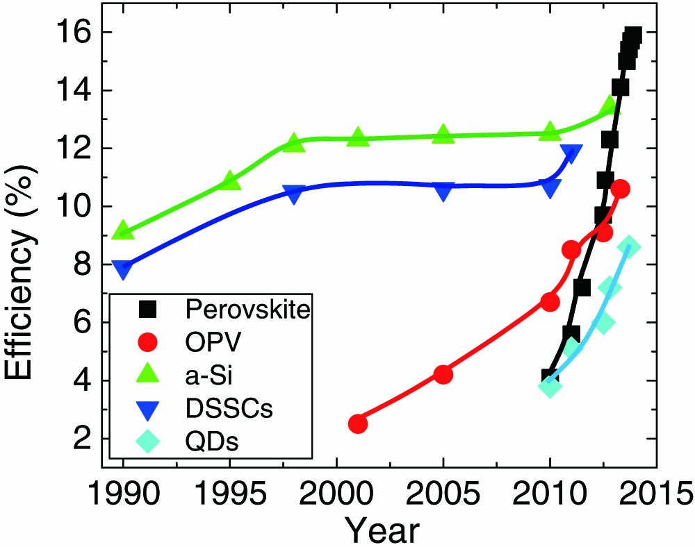
Fig. 1. Efficiency evolution of different thin-film photovoltaic technologies.
![Unit cell of basic ABX3 perovskite structure. The BX6 corner-sharing octahedra are evidenced. Adapted with permission from Ref. [70].](/richHtml/prj/2014/2/5/05000111/img_002.jpg)
Fig. 2. Unit cell of basic AB X 3 perovskite structure. The B X 6 corner-sharing octahedra are evidenced. Adapted with permission from Ref. [70].

Fig. 3. Architecture schematics of three types of photoanodes in perovskite solar cells: (a) mesoporous TiO 2 / Al 2 O 3 / ZrO 2 , (b) TiO 2 / ZnO NWs, and (c) without the scaffold layer.
![(a) UV-Vis absorbance of the FAPbIyBr3−y perovskite with varying y, measured in an integrating sphere. (b) Corresponding steady-state photoluminescence spectra for the same films. (c) Photographs of the FAPbIyBr3−y perovskite films with y increasing from 0 to 1 (left to right). Adapted with permission from Ref. [59].](/Images/icon/loading.gif)
Fig. 4. (a) UV-Vis absorbance of the FAPb I y B r 3 − y perovskite with varying y, measured in an integrating sphere. (b) Corresponding steady-state photoluminescence spectra for the same films. (c) Photographs of the FAPb I y B r 3 − y perovskite films with y increasing from 0 to 1 (left to right). Adapted with permission from Ref. [59].
![Cross-sectional SEM images under lower magnification of completed solar cells constructed from (a) vapor-deposited perovskite film and (b) solution-processed perovskite film. (c) Schematic of dual-source thermal evaporation system for depositing the perovskite absorbers; the organic source was methylammonium iodide, and the inorganic source was PbCl2. (d) Current-density/voltage curves of the best-performing solution-processed (blue lines, triangles) and vapor-deposited (red lines, circles) p-i-n perovskite solar cells measured under simulated AM1.5 sunlight of 101 mW cm−2 irradiance (solid lines) and in the dark (dashed lines). Adapted with permission from Ref. [32].](/Images/icon/loading.gif)
Fig. 5. Cross-sectional SEM images under lower magnification of completed solar cells constructed from (a) vapor-deposited perovskite film and (b) solution-processed perovskite film. (c) Schematic of dual-source thermal evaporation system for depositing the perovskite absorbers; the organic source was methylammonium iodide, and the inorganic source was PbC l 2 . (d) Current-density/voltage curves of the best-performing solution-processed (blue lines, triangles) and vapor-deposited (red lines, circles) p-i-n perovskite solar cells measured under simulated AM1.5 sunlight of 101 mW cm − 2 irradiance (solid lines) and in the dark (dashed lines). Adapted with permission from Ref. [32].
![(a) Photo image of flexible perovskite solar cells on the PET/ITO substrate and (b) device performance of the perovskite solar cells on the PET/ITO flexible substrate before and after bending. Adapted with permission from Ref. [60].](/Images/icon/loading.gif)
Fig. 6. (a) Photo image of flexible perovskite solar cells on the PET/ITO substrate and (b) device performance of the perovskite solar cells on the PET/ITO flexible substrate before and after bending. Adapted with permission from Ref. [60].
![Time-resolved PL measurements taken at the peak emission wavelength of (a) mixed-halide perovskite and (b) triiodide perovskite with an electron (PCBM, blue triangles) or hole (spiro-OMeTAD, red circles) quencher layer, along with stretched exponential fits to the PMMA data (black squares) and fits to the quenching samples by using the diffusion model described in the text. A pulsed (0.3 to 10 MHz) excitation source at 507 nm with a fluence of 30 nJ/cm2 impinged on the glass substrate side. (Inset) Comparison of the PL decay of the two perovskites (with PMMA) on a longer time scale, with lifetimes τe quoted as the time taken to reach 1/e of the initial intensity. Adapted with permission from Ref. [62].](/Images/icon/loading.gif)
Fig. 7. Time-resolved PL measurements taken at the peak emission wavelength of (a) mixed-halide perovskite and (b) triiodide perovskite with an electron (PCBM, blue triangles) or hole (spiro-OMeTAD, red circles) quencher layer, along with stretched exponential fits to the PMMA data (black squares) and fits to the quenching samples by using the diffusion model described in the text. A pulsed (0.3 to 10 MHz) excitation source at 507 nm with a fluence of 30 nJ / cm 2 impinged on the glass substrate side. (Inset) Comparison of the PL decay of the two perovskites (with PMMA) on a longer time scale, with lifetimes τ e quoted as the time taken to reach 1 / e of the initial intensity. Adapted with permission from Ref. [62].
|
Table 1. Summary of the Device Evolution and Performance of Perovskite Solar Cells

Set citation alerts for the article
Please enter your email address