Haoyu Wang, Jun Zheng, Yifei Fu, Chengliang Wang, Xinran Huang, Zhicheng Ye, Liejia Qian, "Multichannel high extinction ratio polarized beam splitters based on metasurfaces," Chin. Opt. Lett. 17, 052303 (2019)
Copy Citation Text
Separating lights into different paths according to the polarization states while keeping their respective path’s polarizations with high purification is keen for polarization multiplex in optical communications. Metallic nanowire gratings with multi-slits in a period are proposed to achieve polarized beam splitters (PBSs) in reflection and diffraction. The setting of multi-slits largely reduces the reflection of photons with a transverse magnetific field via the plasmonic waveguiding effect, which leads to highly polarized output lights with extinction ratio larger than 20 dB in each channel. The proposed reflection/diffraction PBSs enrich the approaches to control the polarization states with the advantages of wide incident angles and flexible beam splitting angles.
Due to the characteristic of breaking through the limitation of the dielectric constant of conventional materials[1], optical metamaterials such as negative index materials and cloaks are able to control the amplitudes and phase of the electromagnetic waves much more flexibly[2–5]. Recently, a two-dimensional metamaterial with subwavelength thickness, i.e., a metasurface, has been increasingly emphasized for its compact structure, low loss, and feasible fabrication process[6]. By an appropriate design, strong resonances compared to three-dimensional materials can also occur in an ultra thin metasurface. Based on metasurfaces, several devices such as metalens[7,8], meta-hologram[9–11], full-color imaging sensors[12,13], and optical antennas[14–16] have been demonstrated. By digital coding metasurface devices[17,18], even more effective controlling of electromagnetic waves can also be achieved. Recently, by using metasurface structures to generate and maintain the polarization of light for high signal to noise ratios, optical coherent communications are being paid more and more attention[19,20]. For further reducing the difficulty of the process, devices based on one-dimensional (1D) metasurfaces such as chromatic polarizers and polarized beam splitters (PBSs) are proposed[21–23]. Due to the intrinsic plasmonic effects at the metal dielectric interface, PBSs based on 1D metallic metasurfaces have presented a much better extinction ratio (ETR) than that of the all-dielectric metamaterials.
So far, PBSs based on 1D metasurfaces have been mainly focused on the transverse magnetic (TM) transmission/transverse electric (TE) reflection (TM-T/TE-R) channels, i.e., photons with TM polarization (corresponding to -polarization) are transmitted, while the others with the TE field (corresponding to -polarization) are reflected. Previously, we proposed a new kind of PBSs based on 1D bilayer metallic nanowire gratings (BMNGs) with a single slit in each period, which can achieve TM-polarized diffraction and TE-polarized reflection simultaneously[24]. However, the TM diffraction (TM-D)/TE-R PBSs based on 1D BMNGs are difficult to achieve high ETR for both TM and TE channels simultaneously because of the opposite requirements on the width of the slits in the unit cells. With the increase of the slits’ width, both the TM-D and TE diffraction increase, leading to a decrease of ETR in the diffraction channel; by decreasing the slits width, TE diffraction is reduced, while TM reflection is increasing, resulting in the deterioration of ETR in reflection. In order to be used in polarization multiplex (PMX), every polarized channel should be of high ETR for maintaining the accuracy of communication data. In any case, the above reported TM-T/TE-R or TE-R/TM-D PBSs cannot achieve high ETR for both channels simultaneously.
For solving the contradictions, we present a new kind of 1D metallic nanowire grating (MNG) with multi-slits in each pitch, namely, compound grating[25,26]. The device can simultaneously achieve the triple functions of facilitating the diffraction of TM lights, efficiently prohibiting the TE polarization diffraction, and substantially reducing the TM light reflection. By using the gap plasmon waveguide (GPW) mode theory[27,28] and Fabry–Perot (F–P)-like resonance theory[29,30], high ETRs of the zeroth order for TE polarization and or order for TM polarization in a large range of incident angles are demonstrated. Besides the large promotion in the performance of ETR, the multi-slit 1D MNGs release the restriction of the pitch grating, which usually should be subwavelength in the conventional PBSs. It means that we can choose the pitch of the gratings with a large freedom to obtain the desired angles between TE and TM beams, which provides convenience for application of the PBSs.
Sign up for Chinese Optics Letters TOC. Get the latest issue of Chinese Optics Letters delivered right to you!Sign up now
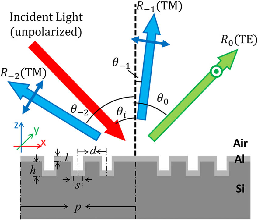
A schematic diagram of the metal compound grating acting as a multichannel reflective optical PBS is presented in Fig. 1. The structure consists of two layers: the bottom silicon layer and top aluminum-film layer. The pitch of the nano-slits’ array is 800 nm. The nano-slits’ height and width are 85 and 55 nm, respectively. The thickness of Al film . The distance between centers of the slits in each period . In addition to the ridge and valley, the sidewall of the nano-slits is also coated by Al with a thickness of 25 nm. The propagation direction of the incident light is parallel to the plane with an incident angle of . The incident light beam is diffracted with angles of , , or , depending on the polarization state: TE-polarized light is reflected with the diffraction order of zeroth; TM-polarized light is diffracted with the order of and .
Figure 1.Schematic drawings of PBSs based on metasurfaces. Unpolarized light (red arrow) is incident on the structure with an angle of and divided into reflected TE (green arrow), and diffracted TM lights (blue arrows) with diffraction angles of , , and , respectively.
In order to investigate the polarization characteristic of the proposed device, the mode effective refractive index of a single nano-slit as a 1D metal–insulator–metal (MIM) waveguide with width is presented in Fig. 2(a), which is calculated by using the following dispersion equation: where is the mode order, is the wave number in vacuum, for TE light, and for TM light. and are the permittivity of the dielectric and metal, respectively. Here, the dielectric is air with , and (Al) is calculated by the Lorantz–Drude mode[31] with the wavelength of . Figure 2(a) shows that the mode exists for all . While the TE mode has a cutoff width as follows: which is 173 nm for the Al/air/Al slit here, thus, a narrow nano-slit with [blue shading in Fig. 2(a)] acts as a PBS. TE light cannot enter into the slit and is reflected almost totally, while TM light can enter into the slit and be diffracted and reflected. Therefore, the incident light is divided into two or three beams: the reflected beam is mainly TE-polarized with , and the and diffracted beams are mainly TM-polarized with and , respectively.
The calculated ETRs of TM and TE light are presented in Fig. 2(b) by using rigorous coupled wave analysis (RCWA) theory. The structural parameters are the same as those in Fig. 1. With the decrease of nano-slit width, of the reflection increased, but of the diffraction decreased. Thus, there is a contradiction between the ETRs of diffracted TM and reflected TE beams. To ensure high ETRs for both reflection and diffraction, we choose .
Figure 2.Numerical simulation of the structure. a, The mode effective refractive index changing with width for MIM waveguide. The blue shading with indicates the region of only the TM mode. b, The reflected (dashed lines) and diffracted (solid lines) changing with the nano-slit width. c, The splitting angle between the reflected and diffracted light beams. Left and right half figures indicate angles between and diffracted TM and reflected TE lights, respectively. d, TM reflected spectra changing with of nano-slits.
The angles between the reflected, diffracted, and diffracted light beams can be tuned by the grating pitch and incident angle , as shown in Fig. 2(c), which are calculated by using the equation where is the order of diffraction. For visible light with a wavelength from 400 to 800 nm, we take with . Thus, the splitting angle between the reflected TE and diffracted TM lights from 30° to 90° and the angle between the reflected TE and diffracted TM lights from 60° to 175° can be obtained. Moreover, the diffraction exists even for the small incident angle (), which ensures that the device can work as a PBS with the wide range of incident angles. With a small grating pitch (e.g., , with ), the device only has two out channels with reflected TE and diffracted TM lights.
With such a thin slit and large pitch, the slit array can produce efficient TE-R and TM-D simultaneously. TM light can enter into the slits and be obviously tuned by the F–P-like cavity effect, as shown in the simulated TM reflected spectrum with in Fig. 2(d). The resonance wavelengths are decided by the F–P formula: where is the effective refractive index of the TM mode, is an additional phase shift, and is the order of the mode. To obtain the low TM reflectance with broadband, we take , shown with a white dashed line in Fig. 2(d).
Simulated spectra and ETR are presented in Fig. 3. The results show that, in the one-slit case, the diffracted [green dashed lines in Fig. 3(d)] is easily above 400 (26 dB), except for the Wood’s anomalies at wavelengths of 430 and 650 nm[32–34]. Wood’s anomalies deduce TM light with high reflectance and low diffraction, as shown with the blue dashed lines in Figs. 3(a) and 3(b). The reflected is below 5 (7 dB), as shown with the red dashed line in Fig. 3(d), which is deduced mainly by the high TM reflectance [blue dashed line in Fig. 3(a)]. Increasing slit width can greatly decrease TM reflectance and make reflected higher, but the diffracted drops sharply at the same time. It means that the one-slit structure makes it hard to obtain high ETRs in both reflection and diffraction simultaneously.
Figure 3.Simulated reflections and diffractions for one-slit and three-slit MNGs with a pitch of 800 nm under incident angle . a, , , b, , , and, c, , with one (dashed lines) or three slits (solid lines) in each period. The insets in b and c are the simulated electric field for TM and TE light, respectively, for the wavelength of 550 nm and . The white dashed lines indicate the surface profile of the structure, and the white arrows depict the incident light. d, The simulated (red lines), (green lines), and (blue lines) of TE and TM light.
In order to ensure both ETRs at high levels, two slits are added in each period to weaken the effect of Wood’s anomalies and reduce the TM reflection further. The simulated results show that the three-slit case has lower TM reflectance [blue solid line in Fig. 3(a)] and higher TM diffracted efficiency [blue and red solid line in Fig. 3(b)] than the one-slit case, especially for diffraction. Meanwhile, the TE-R and TE diffraction efficiencies do not vary much. TE-R keeps a high ratio [, red solid line in Fig. 3(a)], and TE diffraction keeps a low ratio [, blue and red solid lines in Fig. 3(c)]. As a result, the three-slit device exhibits better polarization selection characteristics in reflection. The efficiencies of and TM-D are around 15% for and affected little by Wood’s anomalies [blue and red solid lines in Fig. 3(b)]. The near-field distributions presented in insets of Figs. 3(b) and 3(c) clearly show that TM light enters into the slits and is localized in the interior of the slit; TE light neglects the effect of the slits and reflects directly.
The reflected and diffracted ETRs in the three-slit case, as shown in Fig. 4, present the larger range of working wavelength and incident angle than the one-slit case. The reflected (10 dB) is for a wavelength range of and an incident angle range of [Fig. 4(a)]. For a wavelength of 542 nm, the ETR can be over 1000 (30 dB) in both reflection and diffraction, simultaneously. The diffracted (30 dB) is for wavelengths of and incident angles of , as shown in Figs. 4(b) and 4(c), which provides a high TM polarization property. For wavelengths of and incident angles of , the reflected (20 dB) and diffracted (30 dB) can be obtained, and the splitting angle between the zeroth and or order output light beams can be changed in or , respectively.
Figure 4.Simulated spectra of ETRs for one-slit and three-slit structures. a, , b, , c, for the three-slit case and, d, , e, , f, for the one-slit case with wavelengths of and incident angles of .
Two devices with pitches of 800 and 600 nm were fabricated for different working ranges as PBSs. The scanning electron microscope (SEM) images of the top and side views of the fabricated devices are shown in Figs. 5(a) and 5(b) for the 800 nm pitch device and Figs. 6(a) and 6(b) for the 600 nm pitch device, respectively. Firstly, the silicon gratings were fabricated by using electron-beam lithography and the deep silicon etching system. Then, the silicon grating was deposited with Al films by using the Denton multi-target magnetic control sputtering system. In the device with grating pitch , there are three slits with in each pitch. The slits’ height , the thickness of the Al layer , and thickness of the sidewall is 25 nm. The dimensions of our fabricated device are . The device provides a high TE polarization rejection property with in an incident angle range of and wavelength range of , as shown in Fig. 5(cIII). The diffracted light has a larger region of high TM polarization property with , as shown in Fig. 5(dIII), which covers the angles from 25° to 60° and the center wavelength of about 560 nm with the bandwidth of above 100 nm. The similar characteristics for diffraction are shown in Fig. 5(e), which demonstrate high () in a large range of incident angles (25° to 60°) and bandwidth (). Higher ETRs can be obtained by reducing the technical difference and surface roughness of the device. The measured results are very consistent with the simulated results. To summarize, the device achieved high ETRs () in a region among angles of 36°–41° and wavelengths of 560–590 nm for the reflected TE and and diffracted TM lights, simultaneously.
Figure 5.SEM images and measured spectra dependent on incident angle for the 800 nm pitch structure. a, Top view and, b, side view of the fabricated sample. c, Measured reflected, cI, TE and, cII, TM spectra and, cIII, for wavelengths of and incident angles of . d and e, Measured diffracted spectra, dI, , dII, , eI, , eII, and, dIII, , eIII, for wavelengths of 400–800 nm and incident angles of . As a note, due to the methods of measurement, the reflection spectrum cannot be measured when the angle between the incidence and reflection is less than 5°.
The structural parameters of the device with pitch are the same as the device of 800 nm pitch, except there are two slits in a period. The measured spectra for the device are shown in Figs. 6(c) and 6(d). Because of the short pitch, this device is suitable for two-beam PBS. The energy of diffraction is mainly concentrated on the order, so the efficiency of the TM-D is obviously increased by about 30% compared with the 800 nm pitch device, as shown in Fig. 6(dII). The beam splitting angle between TE and TM lights can be tuned between 40° and 100°. The structure remains angularly insensitive near the wavelength of 600 nm and has high reflected [Fig. 6(cIII)] and diffracted [Fig. 6(dIII)], which all exceed 20 dB.
Figure 6.SEM images and measured spectra dependent on incident angle for the 600 nm pitch structure. a, Top view and, b, side view of the fabricated sample. c, Measured reflected, cI, TE and, cII, TM spectra and, cIII, for different wavelengths and incident angles of in the visible band. d, Measured diffracted spectra, dI, , dII, , and, dIII, for incident angles of in the visible band.
In summary, we have proposed and demonstrated a kind of PBS based on multi-slit metallic gratings, which can separate TE and TM lights into more than two channels. Via the plasmonic waveguiding effect, the beam splitting occurs in a surface thinner than 100 nm, and thus, can be highly integrated. In experiments, we observed the reflection for TE light and diffraction for TM light, of which both the ETRs exceed 20 dB. Our proposed devices not only increase the ETR compared to traditional PBSs, but also provide the possibility of more flexible PMX in optical communications.
Haoyu Wang, Jun Zheng, Yifei Fu, Chengliang Wang, Xinran Huang, Zhicheng Ye, Liejia Qian, "Multichannel high extinction ratio polarized beam splitters based on metasurfaces," Chin. Opt. Lett. 17, 052303 (2019)