• Laser & Optoelectronics Progress
  • Vol. 58, Issue 23, 2316005 (2021)
Hailin Xu*
Author Affiliations
  • College of Physics and Optoelectronic Engineering, Shenzhen University, Shenzhen , Guangdong 518061, China
  • show less
    DOI: 10.3788/LOP202158.2316005 Cite this Article Set citation alerts
    Hailin Xu. Tunable Plasma Waveguides Cladded by Black Phosphorus/Dielectric Multilayer Structures[J]. Laser & Optoelectronics Progress, 2021, 58(23): 2316005 Copy Citation Text show less
    Schematic of plasma waveguides cladded by black phosphorus/dielectric multilayer structures (the clad layer is black phosphorus/dielectric multilayer structures, and the core layer is the dielectric)
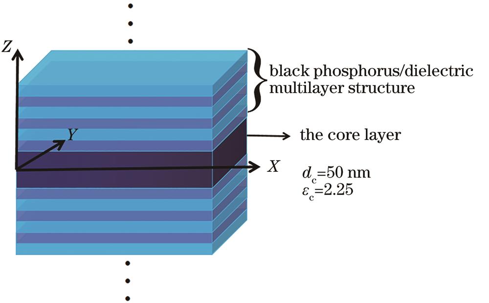
    Fig. 1. Schematic of plasma waveguides cladded by black phosphorus/dielectric multilayer structures (the clad layer is black phosphorus/dielectric multilayer structures, and the core layer is the dielectric)
    Components of effective permittivity in x, y, and z directions of black phosphorus/dielectric multilayer structures. (a) Components of the real part; (b) component of the imaginary part
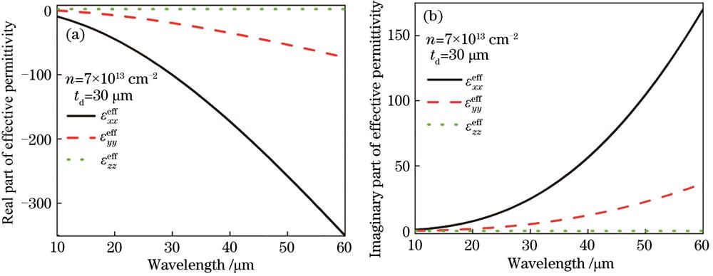
    Fig. 2. Components of effective permittivity in x, y, and z directions of black phosphorus/dielectric multilayer structures. (a) Components of the real part; (b) component of the imaginary part
    Real part of effective permittivity in x direction of black phosphorus/dielectric multilayer structures varied with the wavelength at different electron doping ratesand the dielectric thicknesses of element layer. (a) At different electron doping rates; (b) at different dielectric thicknesses of element layer
    Fig. 3. Real part of effective permittivity in x direction of black phosphorus/dielectric multilayer structures varied with the wavelength at different electron doping ratesand the dielectric thicknesses of element layer. (a) At different electron doping rates; (b) at different dielectric thicknesses of element layer
    Variations of performance of black phosphorus/dielectric multilayer structures plasma waveguides with wavelength at different electron doping rates. (a) Effective refractive index; (b) propagation length; (c) penetration depth; (d) figure of merit (FOM)
    Fig. 4. Variations of performance of black phosphorus/dielectric multilayer structures plasma waveguides with wavelength at different electron doping rates. (a) Effective refractive index; (b) propagation length; (c) penetration depth; (d) figure of merit (FOM)
    Variations of performance of black phosphorus/dielectric multilayer structures plasma waveguides with wavelength at different dielectric thicknesses. (a) Effective refractive index; (b) propagation length; (c) penetration depth; (d) figure of merit
    Fig. 5. Variations of performance of black phosphorus/dielectric multilayer structures plasma waveguides with wavelength at different dielectric thicknesses. (a) Effective refractive index; (b) propagation length; (c) penetration depth; (d) figure of merit
    Distribution of magnetic field amplitude along y direction
    Fig. 6. Distribution of magnetic field amplitude along y direction
    Types of PWGsEffective indexPropagation length /μmPenetration depth /μmFoM
    Metal/dielectric multilayer structures PWGs1.4‒1.510‒205‒1040‒100
    Black phosphorus/dielectric multilayer structures PWGs2‒420‒600.05‒0.07150‒500
    Table 1. Comparison of effective index, propagation length, penetration depth, and figure of merit of two plasma waveguides
    Hailin Xu. Tunable Plasma Waveguides Cladded by Black Phosphorus/Dielectric Multilayer Structures[J]. Laser & Optoelectronics Progress, 2021, 58(23): 2316005
    Download Citation