
Baojuan Dong, Teng Yang, Zheng Han. Flattening is flattering: The revolutionizing 2D electronic systems[J]. Chinese Physics B, 2020, 29(9):
- Chinese Physics B
- Vol. 29, Issue 9, (2020)
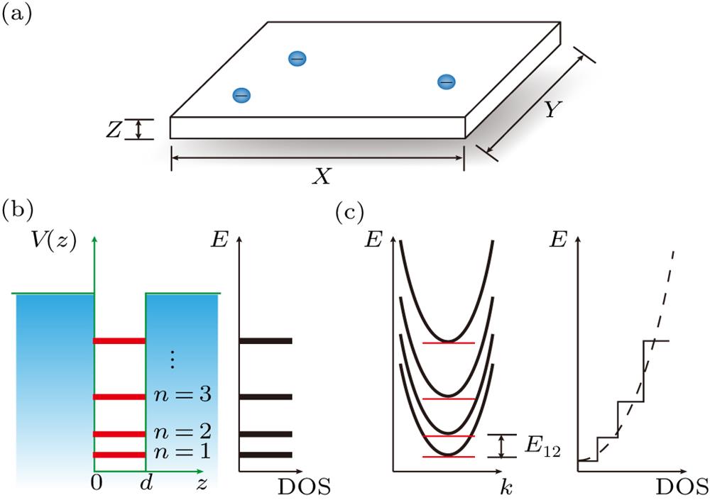
Fig. 1. (a) Schematic 2D structure with z direction confinement. (b) The z -direction confinement spectrum of one-dimensional quantum well model. (c) Band structure and density of states for quasi-two-dimensional electron gas.
![(a) The QHE measured in a 6-nm-thick graphite flake at 0.25 K. (b) Schematic illustrations of electron trajectories under different conditions, (c) Energy gaps for the so-called 2.5D QHE as a function of thickness.[26] Reproduced with permission from Ref. [26].](/richHtml/cpb/2020/29/9/097307/img_2.jpg)
Fig. 2. (a) The QHE measured in a 6-nm-thick graphite flake at 0.25 K. (b) Schematic illustrations of electron trajectories under different conditions, (c) Energy gaps for the so-called 2.5D QHE as a function of thickness.[26 ] Reproduced with permission from Ref. [26 ].
Fig. 3. Schematic illustrations of (a) free 2D electrons, (b) interlayer-interacted 2D electrons, (c) correlated 2D electrons, and (d) twisted 2D electronic systems.
Fig. 4. (a), (b) FeSe monolayer epitaxially grown on SrTiO3(001) substrate, showing superconducting transition temperature above 100 K.[114 ] (c) Schematic picture of transfer process of isolated freestanding SrTiO3 layers.[115 ] (d), (e) Characterizations of the SrTiO3 few unit cells.[115 ] (f)–(h) Superconducting behavior of monolayered BSCCO.[9 ] Reproduced with permission from Refs. [9 ,114 ,115 ].
Fig. 5. Magnetic hysteresis loops measured in a 5-layered MnBi2Te4, with Hall resistance Rxy quantization indicated by dashed lines in (a) and color map of Rxx in (b).[126 ] (c)–(e) Morphology of a Sb-doped MnBi2Te4device with 8 monolayers.[127 ] (f) Phase diagram of Sb-doped MnBi2Te4 in the parameter space of gap energy, doping ratio, and chemical potential.[127 ] Reproduced with permission from Refs. [126 ,127 ].
Fig. 6. (a) Schematic picture of a drag system with two separated 2D electrons. (b) Schematic picture of a GaAs/AlGaAs double quantum well sample.[152 ] (c), (d) Demonstration of Coulomb drag in graphene at zero magnetic field.[147 ] Width of the Hall bar is about 1.5 μm. (e), (f) Super fluid condensate realized in double bilayer graphene drag system.[142 ] The excitonic condensate, indicated by the red arrow, was examined in the top drag layer in a counter flow configuration at ν T = 1. (b)–(f) Reproduced with permission from Refs. [142 ,147 ,152 ].
Fig. 7. (a) Schematic picture of a TBLG. (b) Illustration of the electronic band structure of a flat band (blue) induced by the magic angle moiré superlattice. (c) Schematic picture of the moiré superlattice with their stacking order marked with colors. A full filling of the mini flat band corresponds to 4 electrons in the moiré unit cell originated from the 4-fold degeneracy. (d) Summarization of state-of-the-art experimentally observed correlated quantum states in TBLG with the rotation close to the magic angle.
Fig. 8. (a) Schematic picture of a double gate programmable MoS2 transistor, which is capable to integrate photoswitching logic and memory in a single cell.[205 ] (b) Ballistic avalanche transistor made of InSe/BP heterostructure.[206 ] (c) Ferroelectric domains realized by local patterning and the resulted photo detector with arbitrarily defined shapes.[207 ] (d) A FinFET using monolayered TMDC to replace the conventional Si fin channel.[208 ] Reproduced with permission from Refs. [205 –208 ].


Set citation alerts for the article
Please enter your email address

© Copyright 2018-2021 | Chinese Laser Press. All Rights Reserved 沪ICP备15018463号-20