Abstract
The emission wavelength of InGaN/GaN dot-in-wire LED can be tuned by modifying the nanowire diameter, but it causes mismatched angular distributions between blue, green, and red nanowires because of the excitation of different waveguide modes. Besides, the far-field radiation patterns and light extraction efficiency are typically calculated by center dipoles, which fails to provide accurate results. To address these issues, we first compare the simulation results between central dipole and dipole cloud with experimental data. Next, we calculate and analyze the display metrics for full-color nanowire LEDs by 3D dipole cloud. Finally, we achieve unnoticeable angular color shift within ±20° viewing cone for augmented reality (AR) and virtual reality (VR) displays with an improved light extraction efficiency.The emission wavelength of InGaN/GaN dot-in-wire LED can be tuned by modifying the nanowire diameter, but it causes mismatched angular distributions between blue, green, and red nanowires because of the excitation of different waveguide modes. Besides, the far-field radiation patterns and light extraction efficiency are typically calculated by center dipoles, which fails to provide accurate results. To address these issues, we first compare the simulation results between central dipole and dipole cloud with experimental data. Next, we calculate and analyze the display metrics for full-color nanowire LEDs by 3D dipole cloud. Finally, we achieve unnoticeable angular color shift within ±20° viewing cone for augmented reality (AR) and virtual reality (VR) displays with an improved light extraction efficiency.Introduction
High resolution density, wide field of view (FoV), lightweight and compact formfactor, and low power consumption are demanding requirements for augmented reality (AR) and virtual reality (VR) displays1. Compared to active-matrix liquid crystal displays (LCDs) and organic light-emitting diode (OLED) displays, microLED (μLED) is attracting more ·attention due to its high peak brightness, excellent dark state, high resolution density, small formfactor, and long lifetime2-5. Recently, JBD (Jade Bird Display) announced a 0.22-inch full-color μLED panel with 5K pixels per inch (PPI) by monolithic integration, and the red, green, and blue (R, G, B) sub-pixel pitch is only 2.5 μm. At 2022 Touch Taiwan, PlayNitride also exhibited a 0.49-inch full-color µLED demo with 2.5-µm subpixel size by quantum-dot color conversion and sub-pixel rendering. However, to match with human visual acuity which is 60 pixels per degree (PPD), a PPI of 6.7K is required for a 0.3-inch display panel to offer 40° FoV for AR applications6. To reduce the pixel size further, the increased sidewall defects would dramatically decrease the internal quantum efficiency (IQE), which in turn increases the power consumption7-10. In addition, producing efficient GaN based green and red μLEDs remains a technical challenge11.
Nanowire LEDs show great potential for achieving high resolution density and high external quantum efficiency (EQE) at the same time12-14. In 2018, Aledia reported a nanowire LED12 whose EQE is independent of pitch size when the pitch size is reduced from 1000 μm to 5 μm. For nanowire LEDs with submicron diameter, the IQE can still achieve 58.5%15 and the vertical structure functions as a waveguide to effectively couple the light out16. Additionally, the out-of-plane design can effectively enhance dopant incorporation17, 18, increase heat dissipation19, reduce dislocation density20, 21, and support multi-color monolithic integration22-24. Among different nanowire structures, InGaN/GaN dot-in-wire hexagonal LED is attractive due to its diameter-dependent emission wavelength and excellent electrical performance25. Remarkably, the emission wavelength of the InGaN/GaN nanowire LED depends on its diameter due to the shorter lateral diffusion length of Indium adatom than GaN adatom26. In comparison with small diameter nanowires, the large diameter LED exhibits a reduced Indium adatom incorporation and, therefore, a smaller percentage of Indium existing in its active region, which in turn leads to a shorter emission wavelength. Thus, a full-color display can be achieved by solely changing the nanowire’s diameter. However, these sub-wavelength nanowires exhibit different angular radiation patterns in the far-field, leading to a noticeable angular color shift27. Additionally, the size-dependent waveguide modes are excited in each nanowire so that each one has a different outcoupling efficiency to the environment28. For AR/VR applications, a directional light engine is preferred due to the small etendue of human eye pupil29, 30 whose accepting cone is typically within ±20°. Therefore, the geometry of the nanowire should be optimized to achieve matched radiation patterns for the three primary colors, high light extraction efficiency (LEE), and narrow angular luminance distribution simultaneously.
In this paper, we optimize the InGaN/GaN nanowire LED geometry by 3D dipole cloud through a commercial wave optics simulation software Finite-Difference Time-Domain (FDTD, Ansys inc.). Firstly, we match the InP nanowire’s angular distribution results from 2D dipole cloud simulation with measurement and compare it with traditional central dipole simulation method to validate the accuracy of the model. Secondly, we calculate and analyze the radiation pattern, color gamut, angular color shift, and LEE of full-color InGaN/GaN nanowire LEDs by 3D dipole cloud. Finally, we optimize the nanowire LED by geometrical engineering. After optimization, the angular color shift within the ±20° viewing cone is consistently lower than the human eye’s just-noticeable difference, and the angular full width at half maximum (FWHM) of [blue, green, red] nanowire LEDs is reduced from [48°, 47°, 35°] to [37°, 33°, 24°], while the effective LEE of RGB nanowire LEDs is increased by 7.8%, 36.2%, and 7.4%, respectively.
Results and discussion
Angular distribution matching of InP nanowire LED
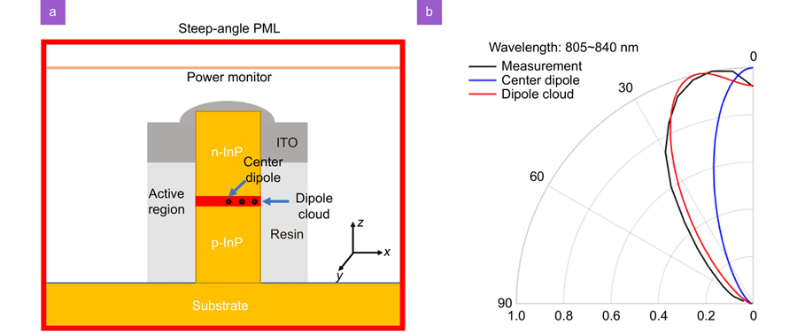
Figure 1(a) shows the 3D FDTD simulation regime and the structure of cylindrical InP nanowire LEDs31. The main body of nanowires is immersed with resin and the top electrode is a transparent indium tin oxide (ITO) film. The FDTD simulation regime is defined by 16 layers of steep-angle perfect matched layer (SA-PML). Detailed simulation parameters are included in Table S1 (Supplementary information). The diameter of the nanowire is 230 nm with 2-μm height which includes a 1.2-μm p-InP layer. The active layer is composed of single layer dipole cloud corresponding to the single quantum well layer. The thickness of resin and top ITO layer is 1.7 μm and 200 nm, respectively. The top of the nanowire is covered with a thin spherical capping of ITO. The dispersion of both InP and ITO is considered32, 33. Due to circular symmetry, three dipoles oscillating along x-, y-, z-direction are simulated separately with a 50-nm spacing along x-direction. Figure 1(b) shows the normalized polar plot comparison of spectrally integrated electroluminescence (EL) between simulated and experimental data from ref.31. The calculation of spectrally and spatially integrated angular distribution by FDTD 2D power monitor will be discussed in detail in Section 2D Angular distribution and LEE calculation. The emission wavelength is 805 nm~840 nm, which is dominated by wurtzite portion of InP nanowire. Therefore, the dipole oscillating along c-axis (z-axis) is weaker than that of the other two. The measured data (black curve) indicates that InP nanowire EL exhibits a batwing profile and the peak intensity locates at ~10°, which is totally different from the response calculated by traditional simulation method (blue curve) that only uses a single dipole in the center of the nanowire. On the other hand, a good agreement between the dipole cloud simulation (red curve) and the measured data is found. A clear batwing profile where the peak intensity takes place at 14° is found, and the minor differences result from inhomogeneous boarding by surface defects. The dipole cloud simulation shows a pronounced accuracy due to the following two reasons. First, the central dipole method ignores the dipoles close to the edge of the active layer(s), which causes a significant mismatch due to the neglect of high-order mode excited by symmetry breaking. Second, the dipoles close to edge of the active layer(s) typically have a heavier geometrical weightage. Consequently, dipole cloud simulation is necessary when calculating the performance of nanowire LEDs whose diameter is larger than 200 nm.

Figure 1.(a) 3D-FDTD InP nanowire LED simulation schematic. (b) Simulated far-field radiation patterns of InP nanowire LED. The experimental data (black curve) included for comparison are from ref.31.
Full-color InGaN/GaN simulation model
Our multicolor single InGaN/GaN dot-in-nanowire LED model is built based on Ra’s experimental results25. As indicated in Fig. 2(a), each nanowire consists of 300-nm n-GaN layer, 60-nm six vertically aligned InGaN/GaN quantum dots layer (active region), 150-nm p-GaN layer, and 150-nm GaN capping layer. The refractive index of the 10-nm Ti mask follows Palik’s handbook34 and the dispersions of GaN and GaN/InGaN active region are calculated by Liu et al35. The nanowire except for the capping is immersed in polyimide whose refractive index is 1.5. The diameter of blue, green, and red nanowires is 630 nm, 420 nm, and 220 nm, respectively. The boundary condition is 16-layer SA-PML to absorb all the escaped light. Hexagonal prism and the capping layer are precisely constructed in the simulation with 10-nm and 5-nm mesh, respectively, along all the x-, y-, and z-directions. Detailed simulation parameters are included in Table S2 (Supplementary information). A large emission box monitor is placed around the structure in the air to calculate the emission power of the LED. The substrate side of the 3D large box monitor is open to get rid of the substrate loss. Small dipole box monitors are placed surrounding each dipole source to calculate the dipole power. Therefore, the light extraction efficiency is calculated by the ratio of the emission power to the dipole power. Besides, the far-field distribution map is captured by the 2D power monitor placed above the structure.
Figure 2.(a) Schematic of FDTD simulation model in x-z plane. (b) Top view of blue hexagonal nanowire LED. (c) Measured EL spectra of single nanowire LEDs with different diameters from ref.25.
In x-y plane, due to the hexagonal structure, dipoles are divided into two directions: short axis and long axis, which are defined by inscribed circle and circumscribed circle, respectively. During each simulation, the long axis dipoles are matched with x-axis initially. Then, the short axis dipoles are matched to x-axis by simply rotating the structure by 30°. Here, we denote this axis dependence to be L and S. Each adjacent dipole is separated by 50 nm. For an example of blue nanowire LED shown in Fig. 2(b), the short axis and long axis consist of 6 and 7 dipoles, respectively. For GaN, its crystal structure is wurtzite36; therefore, the dipoles oscillating along c-axis are neglected and only two polarizations of dipoles are simulated: in-axis and out-of-axis. Here, we denote this axis dependency to be I and O. Due to the hexagonal symmetry condition, a total of 804 dipoles are considered in blue nanowire. For green nanowire LEDs, 4 dipoles are simulated along short axis and 5 dipoles are considered for long axis, which results in a total number of 516 dipoles. For red LEDs, the response of 228 dipoles consisting of 2 dipoles for short axis and 3 dipoles for long axis is calculated. The emission wavelength of dipole sources follows the unfiltered measured emission spectra25 (solid lines in Fig. 2(c)). All the three nanowires without color filters have side lobe emission since the Indium adatom diffusion is difficult to be perfectly controlled. In addition, the red nanowire emission spectrum is relatively broad (FWHM~120 nm) since it is formed by InGaN37. After applying color filters, the side lobes are suppressed significantly, which increases the color purity and therefore enlarges the color gamut. Details will be discussed in Section LEE and near-field distribution maps.
2D Angular distribution and LEE calculation
From FDTD 2D power monitor, the far field distribution A as a function of (θ, φ) is calculated for each wavelength λ, polarization state p (I or O), simulation axis a (L or S), and dipole position (x, z). Firstly, the wavelength and polarization dependencies can be eliminated by considering the spectral average of the source38:
where θ is the polar angle, φ is the azimuthal angle, and S(λ) is the emission spectrum. The simulation axis dependence can be eliminated by separating A1 into long-axis dipoles and short-axis dipoles. In addition, the position independent angular distribution is calculated by integrating the active area in x-y plane and then summing the results together from each active layer. The position-averaged angular distribution for long axis (A2L) and short axis (A2S) can be calculated as:
where RL and RS represent the radius of long-axis dipoles and short-axis dipoles, respectively. Note that in
Eq. (2b), the short axis response should also be normalized by circumscribed circle area for a fair comparison. The total response is the summation of all the dipoles. Here, the angle between long axis and short axis is 30°, and the angle between adjacent long axes is 60°. Therefore, the final angular distribution A3 can be obtained from the summation of all the short- and long-axis dipole responses:
where k describes the in-plane rotation.
The LEE of an LED is defined by the ratio of the emitting power and dipole power. For each dipole, the LEE can be calculated as:
where PE is the total power received by the large emission box monitor and PD is the total power calculated by the small dipole box monitor as shown in Fig. 2(a). Similar to
Eq. (1), the wavelength and polarization state independent LEE can be calculated as:
The position-averaged angular distributions for long- and short-axis dipole responses are:
Here, the short-axis dipole response is normalized by the inscribed circle area because each LEE is calculated separately. The total LEE is the summation of both axis dipole responses:
where BL=
and BS=
are the weightage coefficients for long axis and short axis, respectively.
For AR applications, we define the effective LEE to be the light received within ±20° in the far-field because only the extracted light within this accepting cone can be received by the imaging system. Therefore, the wavelength and polarization state independent effective LEE in
Eq. (5) can be expressed as:
where r is the ±20° spectral coefficient which is calculated as:
The calculation of the rest part is identical to the total LEE as shown in
Eqs. (6–8).
2D Angular distribution and angular color shift
Figure 3(a–c) depict the normalized 2D angular distribution calculated in Section 2D Angular distribution and LEE calculation for blue, green, and red nanowire LEDs, respectively. By summing the results from both long and short axes, the final angular distribution is almost circular symmetric. Among these, the blue nanowire LED (Fig. 3(a)) shows the broadest angular distribution because it has the largest diameter and shortest emission wavelength. Therefore, high-order waveguide modes are excited, which results in a large emission angle from the capping layer. In addition, the peak intensity for green nanowire LED’s angular distribution (Fig. 3(b)) is not located at center. On the other hand, the red nanowire LED (Fig .3(c)) can efficiently concentrate light in the normal direction.
Figure 3.(a–c) Normalized 2D angular distribution for (a) blue, (b) green, and (c) red LEDs. (d) Normalized 1D angular distribution when azimuthal angle φ=0°.
Figure 3(d) depicts the angular distribution of blue, green, and red nanowire LEDs when the azimuthal angle φ=0°. Among these, the angular distribution of green LED shows a batwing profile, and its peak intensity takes place at θ~26°. The FWHM of [blue, green, red] nanowire LEDs is [48°, 47°, 35°], respectively, which are all narrower than Lambertian distribution where the FWHM occurs at 60°. On the other hand, the angular mismatch between RGB nanowire LEDs results in a color shift at different view angles (θ).
Figure 4(a) shows the color gamut of the nanowire LEDs and 18 selected reference colors in Macbeth ColorChecker at 0° viewing angle39. Without applying color filters, the nanowire LED only covers 55.7% DCI-P3 color space and 40.6% Rec.2020. With color filters, the color gamut boosts to 118.5% DCI-P3 and 86.4% Rec.2020. Such a big improvement results from the suppression of side lobe caused by Indium diffusion. Based on 1D angular distribution in Fig. 3(d) and emission spectrum in Fig. 2(c), the angular color shift from 0° to 30° with 1° interval is calculated by our home-made MATLAB code. Figure 4(b) describes the color shift trend for mixing colors because of RGB angular distribution mismatch. As the inset of Fig. 4(b) shows, at ±20° accepting cone, the average color shift is 0.023, which exceeds human eye’s just-noticeable level (∆u'∆v'≤0.02). The issue gets worse as the viewing angle further increases and the average color shift reaches 0.042 at 30° because the RGB color ratio is further increased as shown in Fig. 3(d).
Figure 4.(a) Simulated color triangle of the GaN/InGaN nanowire LED display and CIE coordinates of 18 reference colors at 0° viewing angle. (b) Simulated color shift of 18 reference colors from 0° to 20° viewing angle. Inset: Simulated average color shift from 0° to 30° viewing angle.
LEE and near-field distribution maps
According to
Eqs. (5–7), the total LEE of blue, green, and red nanowire LEDs is calculated to be 22%, 49.5%, and 57%. Besides, the LEE of each dipole is highly dependent on its horizontal direction (x-direction) as shown in Fig. S1 (Supplementary information). These results agree well with previous simulation works38. Due to the broad angular distribution, the effective LEE for blue, green, and red nanowires calculated by
Eq. (8) is reduced to 9.25%, 18.79%, and 33.02%. Near-field distribution maps of long-axis dipoles at the edge of nanowire in Fig. S2 (Supplementary information) also validate the calculated angular distribution and LEE results.
Optimization
For such nanowire LEDs, the angular distribution and LEE are highly dependent on three factors: 1) n-GaN/p-GaN thickness, 2) p-GaN capping layer thickness, and 3) nanowire diameter. The n-GaN/p-GaN thickness determines the interference between the dipole in MQW and the reflection from the substrate, air, and Ti mask; the p-GaN capping thickness decides the outcoupling efficiency, and the diameter controls possible waveguide modes in the nanowire. Since the emission wavelength is highly dependent on the diameter, we focus on optimizing the first two factors. Considering the real application that all electrodes are fabricated at the same height, the main bodies of all nanowires (except the capping) are kept at the same height. In other words, n-GaN and p-GaN hexagonal prism (except the capping) change simultaneously, resulting in a varying vertical position of active layers. Thus, the 2-dimensional optimization is performed by sweeping the vertical position of the active layers with a 10-nm step and thickness of p-GaN capping from 0 to 300 nm with a 30-nm step (Fig. 5). Limited by our computer memory, only the long axis dipoles with x- and y-polarization at the edge of the nanowire will be simulated since they obtain the heaviest geometrical weightage. For RGB nanowires having a different diameter, different optimized geometries are calculated based on following criteria: 1) narrower angular FWHM for a higher light directionality, 2) matched radiation pattern for reducing angular color shift, and 3) higher effective LEE.
Figure 5.(a–c) 2D colormap of angular FWHM as a function of n-GaN thickness and p-GaN capping height: (a) blue, (b) green, and (c) red nanowire LEDs. (d–f) 2D colormap of effective LEE as a function of n-GaN thickness and p-GaN capping height: (d) blue, (e) green, and (f) red nanowire LEDs.
Figure 5(a–c) describes the optimized angular FWHM for each nanowire. The 2D maps indicate that increasing capping height consistently increases the angular FWHM for all the cases because the emission of escaped light is tilted by the capping. In addition, the angular FWHM and the total LEE (Fig. S3, Supplementary information) are both dependent on the n-GaN thickness because excited waveguide modes in the nanowire are very sensitive to its geometrical variation. At a specific n-GaN thickness, the directional radiation mode is constructively interfered with the reflected wave; at the same time, high-order modes could be suppressed by destructive interference. To have a comprehensive understanding on how to improve efficiency, we plot the 2D colormaps of effective LEE based on
Eq. (8) as shown in Fig. 5(d–f). Based on these results, we find the optimal conditions for blue, green, and red nanowire LEDs are: 1) removing the p-GaN capping completely, and 2) setting the n-GaN thickness at 120 nm, 240 nm, and 250 nm, respectively.
Based on the optimized geometry, we repeat the simulation of each case by 3D dipole cloud. Compared to the results in Fig. 3(a–c), a significant improvement is found in the optimized angular distribution as Fig. 6(a–c) shows. Especially for green nanowire (Fig. 6(b)), the batwing profile is suppressed. Figure 6(d) indicates that the angular FWHM of [blue, green, red] nanowire LEDs is reduced from [48°, 47°, 35°] to [37°, 33°, 24°], respectively. In contrast to unoptimized data (solid lines), the optimized angular distribution (dashed lines) shows a better match in the 0°–20° range. However, due to the excitation of higher order modes, a shoulder feature atθ=32° is found in blue nanowire LED. As calculated from
Eq. (8), the effective LEE of blue, green, and red nanowire LEDs increases from [9.3%, 18.8%, 30.6%] to [10.0%, 25.6%, 33.0%], respectively. The enhancement ratio is 7.4% for blue, 36.2% for green, and 7.8% for red, respectively.
Figure 6.(a–c) Normalized 2D angular distribution for optimized (a) blue, (b) green, and (c) red LEDs. (d) Comparison of normalized 1D angular distribution between unoptimized (solid lines) and optimized (dashed lines) nanowire LEDs.
If the blue and green InGaN/GaN nanowire LEDs can achieve 58.5% IQE15 and red nanowire LED can achieve 32.2% IQE40, then the corresponding effective EQE for AR applications will be blue = 5.9%, green = 15.0%, and red = 10.6%. For µLEDs, its EQE decreases as the mesa size decreases due to sidewall defects and surface recombination. This dependency can be relieved by the potassium hydroxide (KOH) passivation treatment on the sidewall41, 42, while this method still requires validation for mass production. In comparison with the size-dependent blue9, 43 and green InGaN µLED43-47 and assuming 100% of the produced light can be coupled into the imaging system, our blue nanowire LED shows a better performance than µLED whose mesa size is smaller than 10 µm as shown in Fig. 7(a). In addition, Fig. 7(b) indicates that the effective LEE of green nanowire LEDs is even higher than that of the 80-µm µLED. Compared to AlGaInP red µLEDs48, our red nanowire LED is more efficient than that with a 20-µm chip size (Fig. 7(c)). Remarkably, in comparison with the 10-µm mesa size, our blue nanowire LED provides a similar brightness, while green and red nanowire LEDs can offer 1.6× and 1.4× higher efficiency, respectively. Therefore, nanowire LEDs show a pronounced higher efficiency than µLED under small pixel size and high resolution density.
Figure 7.Comparison between calculated effective EQE of nanowire LED (horizontal dash lines) with measured EQE of (a) blue InGaN µLEDs from ref.9,43, (b) green InGaN µLEDs from ref.43-47 and (c) red AlGaInP µLEDs from ref.48 as a function of mesa diameter. Vertical dash lines: EQE of µLEDs with 10-µm mesa size.
In contrast to Fig. 4(b), the angular color shift of 18 reference colors after optimization shown in Fig. 8(a) is reduced, especially for green colors because of the suppressed batwing profile. At 20°, the average color shift is reduced from 0.023 to 0.013 and it is not noticeable until θ > 25° ( Fig. 8(b)), which is already beyond the current acceptance cone for AR headsets.
Figure 8.(a) Simulated angular color shift of 18 reference colors from 0° to 20° after optimization. (b) Simulated average color shift from 0° to 30° viewing angle after optimization.
Conclusions
In conclusion, we have optimized full-color InGaN/GaN nanowire LEDs for AR/VR applications by 3D dipole cloud simulation. The simulation method is validated by matching with previous experimental data. By removing the p-GaN capping and modifying the position of active layers, the angular color shift within ±20° viewing cone is suppressed dramatically and the angular FWHM of [blue, green, red] nanowire LEDs is reduced from [48°, 47°, 35°] to [37°, 33°, 24°], respectively, which is favorable for near-eye displays. Meanwhile, the effective LEE of blue, green, and red is enhanced by 7.8%, 36.2%, and 7.4%, respectively.
Acknowledgements
The UCF group is grateful for the financial support of a.u.Vista Inc., and En-Lin Hsiang for valuable discussions.
Y. Z. Qian proposed the original idea and led the project. Z. Y. Yang helped to calculate color gamut and angular color shift. S. T. Wu supervised the project and edited the manuscript.
The authors declare no competing financial interests.
Supplementary information for this paper is available at https://doi.org/10.29026/oes.2022.220021