
Zekun Ma, Tao Lin, Rongjin Zhao, Wanjun Sun, Yan Mu, Yaning Li, Jianan Xie. Research on Thermal Analysis Modeling of Semiconductor Laser Based on Package Prototype[J]. Laser & Optoelectronics Progress, 2021, 58(23): 2314003
- Laser & Optoelectronics Progress
- Vol. 58, Issue 23, 2314003 (2021)
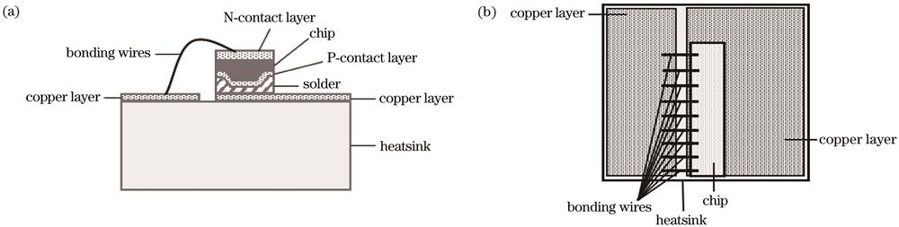
Fig. 1. Schematic diagram of chip and its package structure. (a) Main view; (b) top view
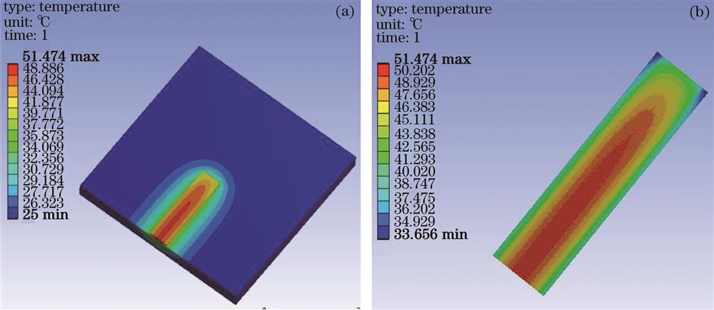
Fig. 2. Results of steady-state thermal simulation of simple model. (a) Overall temperature distribution of model; (b) temperature distribution of active layer
Fig. 3. Temperature distribution results of the simple model. (a) Temperature distribution at the front cavity surface; (b) temperature distribution along the cavity length direction; (c) temperature distribution in the vertical direction of the front cavity surface
Fig. 4. Simulation results of the average temperature of the active layerwith single influeice factor. (a) Stripe width; (b) thickness of copper layer on heat-sink; (c) number of bonding wires
Fig. 5. Ccmparison of simple model and complex model. (a) Simple model; (b) complex model; (c) local enlargement view of internal structure of simple model chip; (d) local enlargement view of internal structure of complex model chip
Fig. 6. Results of steady-state thermal simulation of the complex model. (a) Overall temperature distribution of the model; (b) temperature distribution of the active layer
Fig. 7. Temperabure distribution results of the complex model. (a) Temperature distribution of front cavity surface; (b) temperature distribution along the cavity length direction; (c) temperature distribution in vertical direction of front cavity surfacee
Fig. 8. Output wavelength variation with injection current when the temperature of heat sink bottom surface is 25 ℃ and 50 ℃
Fig. 9. Output wavelength varying with injection current at different heat sink surface temperatures. (a) Heat sink bottom temperature is 25 °C; (b) heat sink bottom temperature is 50 °C
Fig. 10. Device efficiency and device output power with injection current of 10 A. (a) Device efficiency: (b) device output power
Fig. 11. Simulation results and experimental results of average temperature of active layer when the temperature of heat sink bottom surface is 25 ℃ and 50 ℃. (a) Experimental results; (b) simulation results when the temperature of heat sink bottom surface is 25 ℃; (c) simulation results when the temperature of heat sink bottom surface is 50 ℃
Fig. 12. Eror between the experimental results and the simulation results of the two models when the temperature of heat sink bottom surface is 25 ℃ and 50 ℃. (a) Heat sink bottom temperature is 25 ℃; (b) heat sink bottom temperature is 50 ℃
|
Table 1. Structure and material parameters of each layer

Set citation alerts for the article
Please enter your email address
© Copyright 2018-2021 | Chinese Laser Press. All Rights Reserved 沪ICP备15018463号-20