
Tingzhu Wu, Yue Lin, Yu-Ming Huang, Meng Liu, Konthoujam James Singh, Wansheng Lin, Tingwei Lu, Xi Zheng, Jianyang Zhou, Hao-Chung Kuo, Zhong Chen, "Highly stable full-color display device with VLC application potential using semipolar μLEDs and all-inorganic encapsulated perovskite nanocrystal," Photonics Res. 9, 2132 (2021)
- Photonics Research
- Vol. 9, Issue 11, 2132 (2021)
Abstract
1. INTRODUCTION
Owing to their versatility and tunability, microLEDs (μLEDs) with sizes less than 50 μm are considered integral components of next-generation display technology and are able to satisfy the demands of sophisticated devices, such as cellphones, smart watches, virtual reality, microprojectors, and ultra-high-definition TVs [1,2]. Over the past decade, the number of commercially available μLED displays has grown significantly, as manufacturers seek to capitalize on the success of this technology [3]. μLEDs have the potential to surpass organic LEDs by providing displays with high contrast, a wide color gamut, high efficiency, and a wide viewing angle, which are additional to the prospect of translucent and versatile displays [4]. Huang Chen
Perovskite NCs (PNCs), especially those that are lead-based, demonstrate significant advantages over conventional semiconductor NC systems, attracting extensive interest from researchers and manufacturers seeking to produce cost-effective and wide-color-gamut displays [12,13]. Nevertheless, PNCs have some drawbacks. They have, for example, exhibited vulnerability under ambient conditions, particularly in the case of red-emitting PNCs that contain iodine [14]. Water vapor, oxygen, high temperature, and light irradiation cause alteration to the crystal structures of PNCs, typically resulting in photoluminescence (PL) quenching [15]. Several approaches have been explored to enhance the stability of PNCs, among which the most straightforward one is to encapsulate the PNCs in polymer or inorganic shells, thereby preventing the infiltration of water vapor and oxygen [16]. However, polymers are also vulnerable under blue light irradiation, which is inevitable in display technologies [17]. To address this issue, all-inorganic silica encapsulation is adopted for both red and green PNCs in this work, resulting in excellent stability under ambient conditions and, specifically, in response to blue light irradiation.
Even if full-color displays are achieved, the stability of color performance still must be considered. Because of the quantum-confined Stark effect (QCSE), the emitting wavelength of the μLED can shift dramatically under different operating currents [18]. This color shift induced by QCSE is unfavored in display applications, such as mobile phones or laptops, which typically need to operate under different lighting conditions. The wavelength shift can be generated when adjusting the intensity of the display brightness, thereby affecting its color performance. To address these problems, the conventional c-plane μLED can be replaced with nonpolar or semipolar μLEDs that have less QSCE and can thereby achieve a smaller color shift [19]. Huang Chen
Sign up for Photonics Research TOC. Get the latest issue of Photonics Research delivered right to you!Sign up now
In addition to displays, μLEDs have recently been adopted as transmitters in visible light communications (VLC) systems because of their quick response time [21]. Being incorporated with ultraviolet (UV) LEDs, the
At present, there is a paucity of research on μLEDs that are suitable for both displays and VLC. In this study, we present a PNC–μLED device for a full-color display that is developed using a semipolar (20–21) blue μLED array with green-emitting
2. RESULTS
In this study, semipolar GaN was grown using an orientation-controlled epitaxy process on a patterned sapphire substrate (PSS). Details on the PSS and bulk GaN epitaxy can be found in our previous research [20]. In Fig. 1(a), the Xiamen University and National Chiao Tung University logos are visible, over which a 4-inch semipolar (20–21) LED epitaxial wafer and a 2-inch c-plane epitaxial wafer are placed. For both wafers, the high degree of transparency indicates their uniformity and low defect density. Large-area, low-cost epitaxial technology aims to improve the potential of semipolar LEDs for large-scale manufacturing. Figure 1(b) shows the SEM image of the LED epitaxial layer, with labels indicating the crystalline planes of GaN with a normal surface orientation toward (20–21) GaN. In a previous study, Ge doping was found to modify the N-polar (000–1) facet growth rate and decelerate the (101–1) growth rate, resulting in the removal of stacking faults produced in the (000–1) facets [29]. Relative to growth rates reported for c-plane epitaxy, these reported growth rates imply that the crystallinity of the bulk GaN substrate is highly uniform.
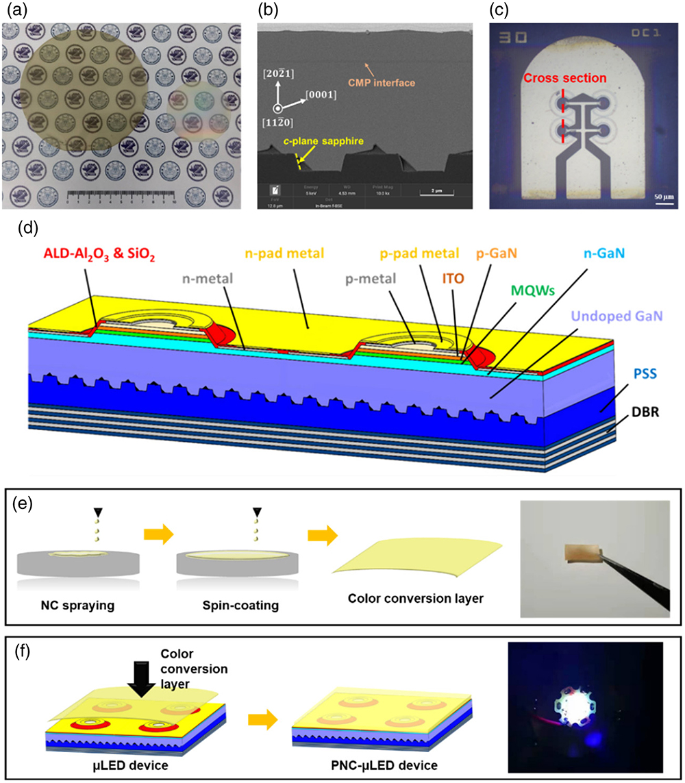
Figure 1.(a) 4-inch semipolar (20−21) blue LED epitaxial wafer and 2-inch commercially available c-plane InGaN/GaN LED wafer with its rear side polished; (b) SEM image showing a cross-sectional view of the semipolar LED epitaxial wafer; (c) optical microscopic image of the 30 μm μLED array sample; schematic diagrams of (d) the semipolar (20−21) μLED structures, (e) the fabrication process and a photo of the color conversion layer, and (f) proposed PNC–μLED device.
The following processes were implemented to fabricate the μLEDs. First, we deposited a 200 nm thick layer of indium tin oxide (ITO) on top of the epitaxial structure of the LEDs. Then, we used a hydrochloric acid solution in conjunction with an inductively coupled plasma reactive ion etching (ICP–RIE) machine to etch a mesa with a depth of approximately 1 μm into the ITO layer. The μLED samples were annealed at 500°C for 2 min in pure nitrogen via a rapid thermal process to produce the optimized p-type ohmic contact. We used lithography and an electron gun, respectively, to pattern and deposit n-metal contacts, which consist of a Ti/Al/Ti/Au structure with a total thickness of 280 nm (comprising 20, 150, 10, and 100 nm layers, respectively). Moreover, atomic layer deposition (ALD)/plasma-enhanced chemical vapor deposition (PECVD) processes are used. A 30 nm thick aluminum oxide passivation layer was grown by trimethylaluminum and
For any fluorescent material, efficiency and stability are two key properties with equal importance. The former represents the instantaneous energy conversion rate, while the latter represents the longevity of the energy conversion efficiency. Based on our experience,
The structural and surface characteristics of the
![]()
Figure 2.XRD patterns of the
The crystal morphology was shown using high-resolution TEM images at 800,000 magnification, and the specific lattice spacing was measured. Figures 3(a) and 3(c) show the TEM images of the
![]()
Figure 3.TEM images of (a)
![]()
Figure 4.EDS element maps of (a)
To answer these two questions, we may consider the formation of PNCs during the high-temperature sintering process. Before sintering, these pores are filled with precursor ions. When the sintering temperature reaches 600°C, the microstructure of MCM-41 collapses, whereby the mesoporous MSs are turned into solid
The fabrication process is different from those also employing
Figures 5(a) and 5(b) display the absorption and PL spectra of the two types of PNC samples under UV excitation (365 nm). The PL emission wavelengths are 660 nm for
![]()
Figure 5.UV-vis absorption and PL spectra of (a)
Figure 6 illustrates the optical and electrical characteristics of the μLED array device. The current density-voltage (J-V) characteristics of the semipolar (20–21) blue μLED array with a chip diameter of 30 μm is shown in Fig. 6(a); the inset represents the optical image of the illuminated semipolar μLED array. The device has a forward turn-on voltage of 3.6 V with a maximum applied current density of
![]()
Figure 6.(a) Current density–voltage (
In addition, the optical polarization characteristics of the semipolar μLED array, which are key features for display applications, are studied. Many studies report that semipolar or nonpolar μLEDs exhibit a high polarization ratio owing to their anisotropic polarized emission, which is an advantage compared with c-plane devices [35,36]. Figure 7(a) displays the maximum and minimum intensities of the polarized light emission from a semipolar array comprising four 30 μm μLEDs, with the result resembling a cosine function. The polarization ratio (
![]()
Figure 7.(a) Polarization characteristics of the
Next, the VLC performance of the PNC–μLED was studied, as shown in Fig. 8. The modulation bandwidth measurement was performed using a vector network analyzer (VNA; Keysight E5071C). As shown in Fig. 8(a), a bias tee (11612A, 45 MHz–26.5 GHz) combines AC signals from the VNA with DC signals from the current source and applies it to the PNC–μLED, which was probed by a high-speed microprobe (ACP40-GS-250, DC–40 GHz). The PNC bandwidth is approximately tens of MHz, which is considerably lower than that of the μLED. Therefore, a filter is used to remove the red and green light generated by PNCs in the experiment [27]. The blue light passing through the filter was collected using an optical fiber, which was coupled with an avalanche photodiode (APD) (SPA-3, DC–2 GHz). The converted signal was traced back to the VNA, where the modulation bandwidth was measured. Figure 8(b) shows the frequency response of the PNC–μLED, revealing that the 3 dB bandwidth increases, owing to the higher injected carrier density in the active region as the injection current increases. This results in a built-in electric field and decreased carrier lifetime. The highest 3 dB bandwidth was measured as 655 MHz, corresponding to an injection current of 200 mA (current density of
![]()
Figure 8.(a) Schematic diagram for bandwidth measurement; (b) frequency response for the PNC–μLED; (c) schematic diagram for the eye diagram measurement; (d)–(f) eye diagrams of the PNC–μLED at 1.0, 1.2, and 1.5 Gb/s, respectively.
![]()
Figure 9.(a) Color gamut of the PNC–μLED under different current densities; and (b) color shift of blue semipolar μLEDs under different current densities.
Figure 9 presents the performance of the PNC–μLED for the display backlight application under different current densities between 2.55 and
Therefore, the device proposed in this study could be used for display applications when operated at low current densities, while at high current densities it could be used for VLC applications. If the device is required for display and communications simultaneously, for the safety of the user’s eyes, the device should work at the low current density region, which is below
3. DISCUSSION
Highly stable PNCs were manufactured with a
4. MATERIALS AND METHODS
A. Synthesis of
A precursor solution was prepared by mixing a particular amount of precursor salts with MCM-41 molecular sieve (masses are listed in Table 1) and dispersing this mixture in 25 mL of purified water. Next, the precursor solution was subjected to ultrasonic vibration for 20 min and stirred vigorously for 10 min to improve dispersion. The precursor solution was transferred to a crucible and placed in a tube furnace filled with high purity Ar gas. The temperature of the tube furnace was first raised to 200°C, and it was maintained for 1 h to evaporate the water. Then, continuous sintering was performed at a temperature of 750°C for 30 min with an Ar flow rate of 15 mL/min. Subsequently, the samples were cooled to room temperature under Ar protection, during which their colors gradually changed, finally crystallizing into PNCs. The final
Precursor Masses
| Samples | CsBr (g) | MCM-41 | ||
|---|---|---|---|---|
| 0.73 | 1.59 | 0 | 2.00 | |
| 0.73 | 0 | 1.27 | 2.00 |
B. Synthesis of PNC
We followed a typical ligand-assisted reprecipitation method (LARP). We mixed CsBr (0.2 mmol) with
C. Synthesis of PNC
This sample was fabricated using the traditional hot injection strategy (HIS) in a two-step process.
Step I: Preparation of Cs-oleate precursor. 0.407 g of
Step II: Synthesis of PNC
D. Fabrication of PNC-
In this process, 0.03 g of
Acknowledgment
Acknowledgment. The authors thank Prof. Rong Zhang and Prof. Rongjun Xie of Xiamen University, Prof. Jung Han of Yale University, Prof. Chi-Wai Chow of Taiwan Chiao Tung University, and Prof. Gong-Ru Lin of Taiwan University for their advice and technical support. We also appreciate the contributions to experimental work, manuscript editing, and constructive discussions from Guolong Chen, Zeping Wang, Zhibin Shangguan, Weizhi Huang, Youcai Deng, Xiaotong Fan, and Xiao Yang of the Solid-state Lighting Laboratory, Xiamen University.
References
[1] C. Chang, K. Bang, G. Wetzstein, B. Lee, L. Gao. Toward the next-generation VR/AR optics: a review of holographic near-eye displays from a human-centric perspective. Optica, 7, 1563-1578(2020).
[2] Y.-M. Huang, K. J. Singh, A.-C. Liu, C.-C. Lin, Z. Chen, K. Wang, Y. Lin, Z. Liu, T. Wu, H.-C. Kuo. Advances in quantum-dot-based displays. Nanomaterials, 10, 1327(2020).
[3] T. Wu, C.-W. Sher, Y. Lin, C.-F. Lee, S. Liang, Y. Lu, S.-W. H. Chen, W. Guo, H.-C. Kuo, Z. Chen. Mini-LED and micro-LED: promising candidates for the next generation display technology. Appl. Sci., 8, 1557(2018).
[4] S.-W. Huang Chen, C.-C. Shen, T. Wu, Z.-Y. Liao, L.-F. Chen, J.-R. Zhou, C.-F. Lee, C.-H. Lin, C.-C. Lin, C.-W. Sher, P.-T. Lee, A.-J. Tzou, Z. Chen, H.-C. Kuo. Full-color monolithic hybrid quantum dot nanoring micro light-emitting diodes with improved efficiency using atomic layer deposition and nonradiative resonant energy transfer. Photon. Res., 7, 416-422(2019).
[5] Y. Huang, E.-L. Hsiang, M.-Y. Deng, S.-T. Wu. Mini-LED, micro-LED and OLED displays: present status and future perspectives. Light Sci. Appl., 9, 105(2020).
[6] J. Cho, J. H. Park, J. K. Kim, E. F. Schubert. White light-emitting diodes: history, progress, and future. Laser Photon. Rev., 11, 1600147(2017).
[7] D. Hwang, A. Mughal, C. Pynn, S. Nakamura, S. Denbaars. Sustained high external quantum efficiency in ultrasmall blue III-nitride micro-LEDs. Appl. Phys. Express, 10, 032101(2017).
[8] X. Wang, Z. Bao, Y.-C. Chang, R.-S. Liu. Perovskite quantum dots for application in high color gamut backlighting display of light-emitting diodes. ACS Energy Lett., 5, 3374-3396(2020).
[9] C.-H. Lin, A. Verma, C.-Y. Kang, Y.-M. Pai, T.-Y. Chen, J.-J. Yang, C.-W. Sher, Y.-Z. Yang, P.-T. Lee, C.-C. Lin, Y.-C. Wu, S. K. Sharma, T. Wu, S.-R. Chung, H.-C. Kuo. Hybrid-type white LEDs based on inorganic halide perovskite QDs: candidates for wide color gamut display backlights. Photon. Res., 7, 579-585(2019).
[10] C. C. Lin, R.-S. Liu. Advances in phosphors for light-emitting diodes. J. Phys. Chem. Lett., 2, 1268-1277(2011).
[11] Z. Liu, C.-H. Lin, B.-R. Hyun, C.-W. Sher, Z. Lv, B. Luo, F. Jiang, T. Wu, C.-H. Ho, H.-C. Kuo, J.-H. He. Micro-light-emitting diodes with quantum dots in display technology. Light Sci. Appl., 9, 83(2020).
[12] J. A. Steele, H. Jin, I. Dovgaliuk, R. F. Berger, T. Braeckevelt, H. Yuan, C. Martin, E. Solano, K. Lejaeghere, S. M. J. Rogge, C. Notebaert, W. Vandezande, K. P. F. Janssen, B. Goderis, E. Debroye, Y.-K. Wang, Y. Dong, D. Ma, M. Saidaminov, H. Tan, Z. Lu, V. Dyadkin, D. Chernyshov, V. Van Speybroeck, E. H. Sargent, J. Hofkens, M. B. J. Roeffaers. Thermal unequilibrium of strained black CsPbI3 thin films. Science, 365, 679-684(2019).
[13] S. Masi, A. F. Gualdrón-Reyes, I. Mora-Seró. Stabilization of black perovskite phase in FAPbI3 and CsPbI3. ACS Energy Lett., 5, 1974-1985(2020).
[14] Y. Wei, Z. Cheng, J. Lin. An overview on enhancing the stability of lead halide perovskite quantum dots and their applications in phosphor-converted LEDs. Chem. Soc. Rev., 48, 310-350(2019).
[15] Z. Shangguan, X. Zheng, J. Zhang, W. Lin, W. Guo, C. Li, T. Wu, Y. Lin, Z. Chen. The stability of metal halide perovskite nanocrystals–a key issue for the application on quantum-dot-based micro light-emitting diodes display. Nanomaterials, 10, 1375(2020).
[16] L. Shi, L. Meng, F. Jiang, Y. Ge, F. Li, X. G. Wu, H. Zhong.
[17] M. C. C. d. Oliveira, A. S. A. C. Diniz, M. M. Viana, V. d. F. C. Lins. The causes and effects of degradation of encapsulant ethylene vinyl acetate copolymer (EVA) in crystalline silicon photovoltaic modules: a review. Renew. Sustain. Energy Rev., 81, 2299-2317(2018).
[18] T. Takeuchi, S. Sota, M. Katsuragawa, M. Komori, H. Takeuchi, H. Amano, I. Akasaki. Quantum-confined stark effect due to piezoelectric fields in GaInN strained quantum wells. Jpn. J. Appl. Phys., 36, L382-L385(1997).
[19] S.-W. H. Chen, Y.-M. Huang, Y.-H. Chang, Y. Lin, F.-J. Liou, Y.-C. Hsu, J. Song, J. Choi, C.-W. Chow, C.-C. Lin, R.-H. Horng, Z. Chen, J. Han, T. Wu, H.-C. Kuo. High-bandwidth green semipolar (20-21) InGaN/GaN micro light-emitting diodes for visible light communication. ACS Photon., 7, 2228-2235(2020).
[20] S.-W. H. Chen, Y.-M. Huang, K. J. Singh, Y.-C. Hsu, F.-J. Liou, J. Song, J. Choi, P.-T. Lee, C.-C. Lin, Z. Chen, J. Han, T. Wu, H.-C. Kuo. Full-color micro-LED display with high color stability using semipolar (20-21) InGaN LED and quantum-dot photoresist. Photon. Res., 8, 630-636(2020).
[21] K. James Singh, Y.-M. Huang, T. Ahmed, A.-C. Liu, S.-W. Huang Chen, F.-J. Liou, T. Wu, C.-C. Lin, C.-W. Chow, G.-R. Lin, H.-C. Kuo. Micro-LED as a promising candidate for high-speed visible light communication. Appl. Sci., 10, 7384(2020).
[22] C. H. Kang, I. Dursun, G. Liu, L. Sinatra, X. Sun, M. Kong, J. Pan, P. Maity, E.-N. Ooi, T. K. Ng, O. F. Mohammed, O. M. Bakr, B. S. Ooi. High-speed colour-converting photodetector with all-inorganic CsPbBr3 perovskite nanocrystals for ultraviolet light communication. Light Sci. Appl., 8, 94(2019).
[23] S. Zhang, D. Tsonev, S. Videv, S. Ghosh, G. A. Turnbull, I. D. W. Samuel, H. Haas. Organic solar cells as high-speed data detectors for visible light communication. Optica, 2, 607-610(2015).
[24] S. Mei, X. Liu, W. Zhang, R. Liu, L. Zheng, R. Guo, P. Tian. High-bandwidth white-light system combining a micro-LED with perovskite quantum dots for visible light communication. ACS Appl. Mater. Interfaces, 10, 5641-5648(2018).
[25] P. Tian, X. Liu, S. Yi, Y. Huang, S. Zhang, X. Zhou, L. Hu, L. Zheng, R. Liu. High-speed underwater optical wireless communication using a blue GaN-based micro-LED. Opt. Express, 25, 1193-1201(2017).
[26] G. Kozlowski, S. Schulz, B. Corbett. Polarization matching design of InGaN-based semi-polar quantum wells—a case study of (11–22) orientation. Appl. Phys. Lett., 104, 051128(2014).
[27] D. Rosales, B. Gil, T. Bretagnon, B. Guizal, F. Zhang, S. Okur, M. Monavarian, N. Izyumskaya, V. Avrutin, Ü. Özgür, H. Morkoç, J. H. Leach. Excitonic recombination dynamics in non-polar GaN/AlGaN quantum wells. J. Appl. Phys., 115, 073510(2014).
[28] H. Zhang, P. Li, H. Li, J. Song, S. Nakamura, S. P. Denbaars. High polarization and fast modulation speed of dual wavelengths electroluminescence from semipolar (20-21) micro light-emitting diodes with indium tin oxide surface grating. Appl. Phys. Lett., 117, 181105(2020).
[29] J. Song, J. Choi, C. Zhang, Z. Deng, Y. Xie, J. Han. Elimination of stacking faults in semipolar GaN and light-emitting diodes grown on sapphire. ACS Appl. Mater. Interfaces, 11, 33140-33146(2019).
[30] Q. Zhang, B. Wang, W. Zheng, L. Kong, Q. Wan, C. Zhang, Z. Li, X. Cao, M. Liu, L. Li. Ceramic-like stable CsPbBr3 nanocrystals encapsulated in silica derived from molecular sieve templates. Nat. Commun., 11, 31(2020).
[31] C. Sun, Y. Zhang, C. Ruan, C. Yin, X. Wang, Y. Wang, W. W. Yu. Efficient and stable white LEDs with silica-coated inorganic perovskite quantum dots. Adv. Mater., 28, 10088-10094(2016).
[32] H.-C. Wang, S.-Y. Lin, A.-C. Tang, B. P. Singh, H.-C. Tong, C.-Y. Chen, Y.-C. Lee, T.-L. Tsai, R.-S. Liu. Mesoporous silica particles integrated with all-inorganic CsPbBr3 perovskite quantum-dot nanocomposites (MP-PQDs) with high stability and wide color gamut used for backlight display. Angew. Chem., 55, 7924-7929(2016).
[33] M. Achermann, M. A. Petruska, S. Kos, D. L. Smith, D. D. Koleske, V. I. Klimov. Energy-transfer pumping of semiconductor nanocrystals using an epitaxial quantum well. Nature, 429, 642-646(2004).
[34] I.-K. Park, M.-K. Kwon, S.-B. Seo, J.-Y. Kim, J.-H. Lim, S.-J. Park. Ultraviolet light-emitting diodes with self-assembled InGaN quantum dots. Appl. Phys. Lett., 90, 111116(2007).
[35] S. E. Brinkley, Y.-D. Lin, A. Chakraborty, N. Pfaff, D. Cohen, J. S. Speck, S. Nakamura, S. P. DenBaars. Polarized spontaneous emission from blue-green m-plane GaN-based light emitting diodes. Appl. Phys. Lett., 98, 011110(2011).
[36] Y. Zhao, S. Tanaka, Q. Yan, C.-Y. Huang, R. B. Chung, C.-C. Pan, K. Fujito, D. Feezell, C. G. V. d. Walle, J. S. Speck, S. P. DenBaars, S. Nakamura. High optical polarization ratio from semipolar (20-2-1) blue-green InGaN/GaN light-emitting diodes. Appl. Phys. Lett., 99, 051109(2011).


Set citation alerts for the article
Please enter your email address

© Copyright 2018-2021 | Chinese Laser Press. All Rights Reserved 沪ICP备15018463号-20