
Tingzhu Wu, Yue Lin, Yu-Ming Huang, Meng Liu, Konthoujam James Singh, Wansheng Lin, Tingwei Lu, Xi Zheng, Jianyang Zhou, Hao-Chung Kuo, Zhong Chen. Highly stable full-color display device with VLC application potential using semipolar μLEDs and all-inorganic encapsulated perovskite nanocrystal[J]. Photonics Research, 2021, 9(11): 2132
- Photonics Research
- Vol. 9, Issue 11, 2132 (2021)
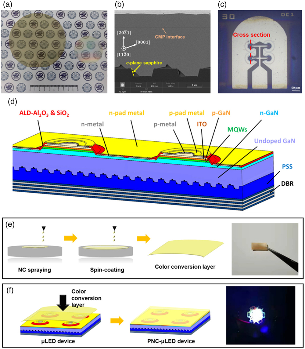
Fig. 1. (a) 4-inch semipolar (20−21) blue LED epitaxial wafer and 2-inch commercially available c-plane InGaN/GaN LED wafer with its rear side polished; (b) SEM image showing a cross-sectional view of the semipolar LED epitaxial wafer; (c) optical microscopic image of the 30 μm μLED array sample; schematic diagrams of (d) the semipolar (20−21) μLED structures, (e) the fabrication process and a photo of the color conversion layer, and (f) proposed PNC–μLED device.
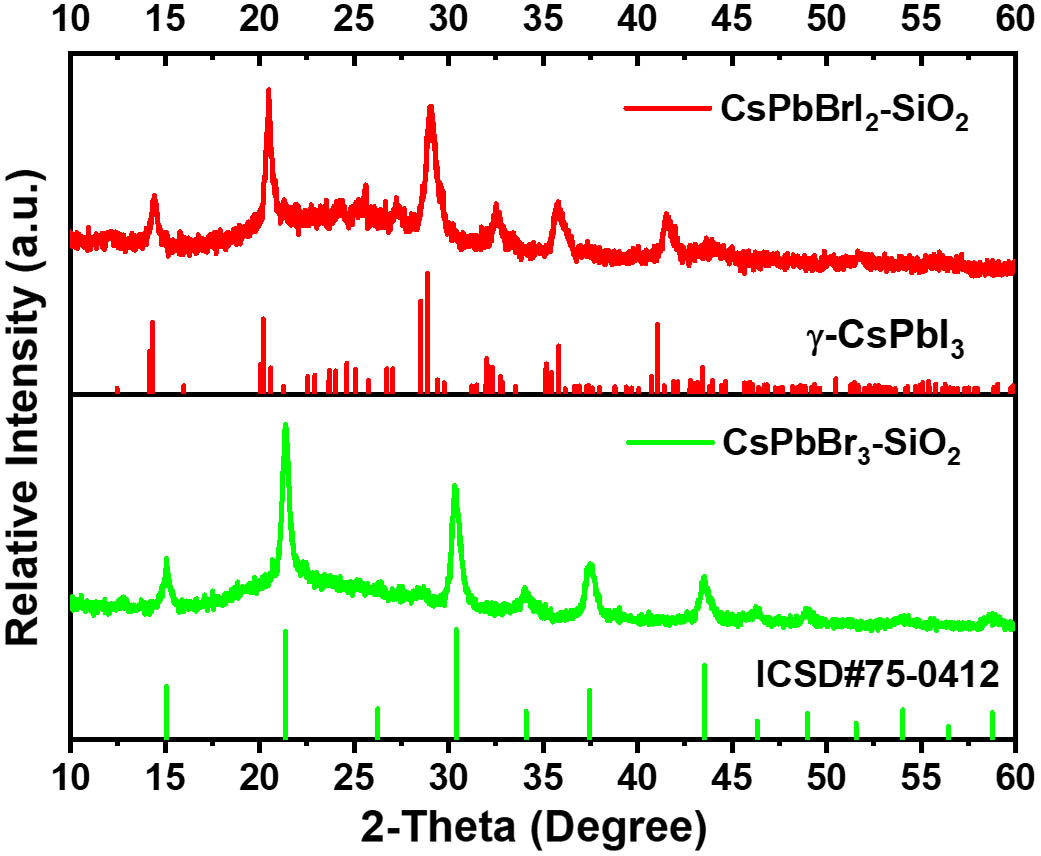
Fig. 2. XRD patterns of the CsPbBrI 2 − SiO 2 CsPbBr 3 − SiO 2
Fig. 3. TEM images of (a) CsPbBr 3 − SiO 2 CsPbBrI 2 CsPbBr 3 − SiO 2 CsPbBrI 2 − SiO 2 CsPbBr 3 CsPbBr 2
Fig. 4. EDS element maps of (a) CsPbBrI 2 − SiO 2 CsPbBr 3 − SiO 2
Fig. 5. UV-vis absorption and PL spectra of (a) CsPbBrI 2 − SiO 2 CsPbBr 3 − SiO 2
Fig. 6. (a) Current density–voltage (J–V ) curve for the 30 μm μLED array and its illuminated image; (b) EL spectra for different injection currents; (c) peak wavelength shift and FWHM as a function of current density; and (d) EQE and emitted power as a function of current density.
Fig. 7. (a) Polarization characteristics of the 30 μm × 4
Fig. 8. (a) Schematic diagram for bandwidth measurement; (b) frequency response for the PNC–μLED; (c) schematic diagram for the eye diagram measurement; (d)–(f) eye diagrams of the PNC–μLED at 1.0, 1.2, and 1.5 Gb/s, respectively.
Fig. 9. (a) Color gamut of the PNC–μLED under different current densities; and (b) color shift of blue semipolar μLEDs under different current densities.
|
Table 1. Precursor Masses

Set citation alerts for the article
Please enter your email address
© Copyright 2018-2021 | Chinese Laser Press. All Rights Reserved 沪ICP备15018463号-20