• Chinese Optics Letters
  • Vol. 21, Issue 3, 033603 (2023)
Lu Zhang, Chao Meng, Hao Yang, and Wending Zhang*
Author Affiliations
  • Key Laboratory of Light Field Manipulation and Information Acquisition, Ministry of Industry and Information Technology, and Shaanxi Key Laboratory of Optical Information Technology, School of Physical Science and Technology, Northwestern Polytechnical University, Xi’an 710129, China
  • show less
    DOI: 10.3788/COL202321.033603 Cite this Article Set citation alerts
    Lu Zhang, Chao Meng, Hao Yang, Wending Zhang. Azimuthal vector beam illuminating plasmonic tips circular cluster for surface-enhanced Raman spectroscopy[J]. Chinese Optics Letters, 2023, 21(3): 033603 Copy Citation Text show less
    (a) Sketch map of one PTCC unit equidistantly surrounded by six other PTCC units; (b) position relationship between one PTCC unit and the six PTCC units equally spaced on a circle; (c) structure parameters of one PTCC unit; transverse electric field component of (d) LPB, (e) RVB, and (f) AVB tightly focused via an micro-objective (MO) with NA = 0.85; scattering spectra of one PTCC unit vertically illuminated via the (g) LPB, (h) RVB, and (i) AVB in the range of 450–700 nm.
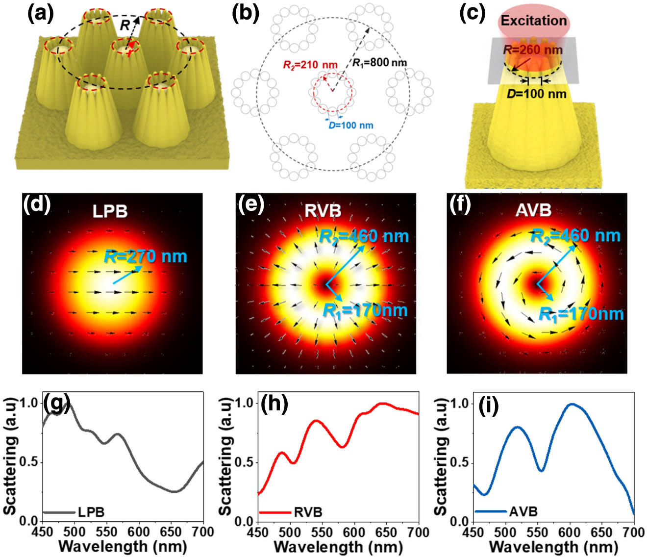
    Fig. 1. (a) Sketch map of one PTCC unit equidistantly surrounded by six other PTCC units; (b) position relationship between one PTCC unit and the six PTCC units equally spaced on a circle; (c) structure parameters of one PTCC unit; transverse electric field component of (d) LPB, (e) RVB, and (f) AVB tightly focused via an micro-objective (MO) with NA = 0.85; scattering spectra of one PTCC unit vertically illuminated via the (g) LPB, (h) RVB, and (i) AVB in the range of 450–700 nm.
    (a)–(c) Sketch maps of the excitation light with three kinds of spatial electric field vectors vertically illuminating the center of one PTCC unit; (d)–(f) electric-field intensity and (g)–(i) charge distributions at the bottom of one PTCC unit when the center of one PTCC unit was illuminated via the focused LPB, RVB, and AVB, respectively.
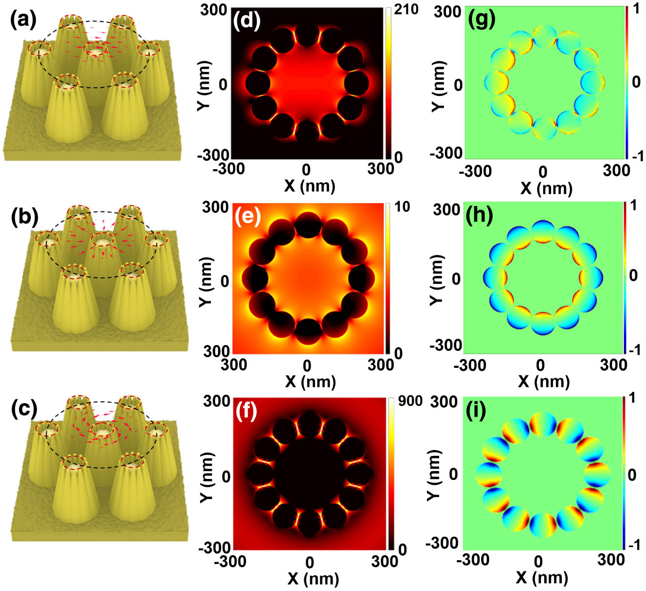
    Fig. 2. (a)–(c) Sketch maps of the excitation light with three kinds of spatial electric field vectors vertically illuminating the center of one PTCC unit; (d)–(f) electric-field intensity and (g)–(i) charge distributions at the bottom of one PTCC unit when the center of one PTCC unit was illuminated via the focused LPB, RVB, and AVB, respectively.
    (a) Sketch maps of the tightly focused LPB, RVB, and AVB vertically illuminated on the center of two adjacent PTCC units; (b)–(d) electric field intensity distributions of the four PTCC units corresponding to LPB, RVB, and AVB illumination, respectively.
    Fig. 3. (a) Sketch maps of the tightly focused LPB, RVB, and AVB vertically illuminated on the center of two adjacent PTCC units; (b)–(d) electric field intensity distributions of the four PTCC units corresponding to LPB, RVB, and AVB illumination, respectively.
    (a) Sketch map of the fabrication process of the PTCC array; (b) SEM image of PTCC array with scale bar of 10 µm; the inset is the microimage of the PTCC array on a 2 cm silicon wafer; (c) SEM image of the PTCC array with scale bar of 800 nm; the inset is one PTCC unit with tip curvature radius of ∼20 nm; (d) measured reflection spectrum (black curve) and the calculated scattering spectrum (red curve) of the PTCC array.
    Fig. 4. (a) Sketch map of the fabrication process of the PTCC array; (b) SEM image of PTCC array with scale bar of 10 µm; the inset is the microimage of the PTCC array on a 2 cm silicon wafer; (c) SEM image of the PTCC array with scale bar of 800 nm; the inset is one PTCC unit with tip curvature radius of ∼20 nm; (d) measured reflection spectrum (black curve) and the calculated scattering spectrum (red curve) of the PTCC array.
    (a) Sketch map of experimental setup for SERS examination; (b) Raman spectra of MG, with concentration from 10−10 M down to 10−13 M, absorbed on the PTCC array and excited via LPB and AVB, respectively; (c) Raman mapping of MG with concentrations of 10−8 M. The inset is the histogram of the intensities of 1587 cm−1 characteristic peak obtained along the white dashed in (c); (d) Raman spectra of MG with concentrations of 10−12 M (red curve) and 10−3 M (black curve) on PTCC and Si substrates, respectively.
    Fig. 5. (a) Sketch map of experimental setup for SERS examination; (b) Raman spectra of MG, with concentration from 10−10 M down to 10−13 M, absorbed on the PTCC array and excited via LPB and AVB, respectively; (c) Raman mapping of MG with concentrations of 10−8 M. The inset is the histogram of the intensities of 1587 cm−1 characteristic peak obtained along the white dashed in (c); (d) Raman spectra of MG with concentrations of 10−12 M (red curve) and 10−3 M (black curve) on PTCC and Si substrates, respectively.
    Lu Zhang, Chao Meng, Hao Yang, Wending Zhang. Azimuthal vector beam illuminating plasmonic tips circular cluster for surface-enhanced Raman spectroscopy[J]. Chinese Optics Letters, 2023, 21(3): 033603
    Download Citation