
Lu Zhang, Chao Meng, Hao Yang, Wending Zhang, "Azimuthal vector beam illuminating plasmonic tips circular cluster for surface-enhanced Raman spectroscopy," Chin. Opt. Lett. 21, 033603 (2023)
- Chinese Optics Letters
- Vol. 21, Issue 3, 033603 (2023)
Abstract
Keywords
1. Introduction
Surface-enhanced Raman spectroscopy (SERS), as a powerful analytical tool to obtain the “fingerprints” information of molecules[1–3], has been widely used in physical, chemical, material, and biological applications. Compared with the traditional Raman spectroscopy, SERS uses the noble metallic nanostructures with plasmon resonance effect at the excitation wavelength to amplify Raman scattering intensity of the molecules. Therefore, tailoring the electric near-field enhancement properties of the metallic nanostructures is critical for improving SERS performance.
So far, various metallic nanostructures, such as nanoparticles[4], nanodisks[5], and nanotips[6], have been proposed for SERS applications. In addition, the plasmonic nanocluster was also proposed for increasing SERS performance, due to possessing the strong electric resonances[7]. These resonance effects of the plasmonic nanocluster arise from the strong electromagnetic coupling between closely spaced plasmonic particles/disks[8], and the plasmonic resonance can be modified by tuning the cluster size, geometry, and interparticle spacing.
Electron beam lithography (EBL) and the self-assembly methods have been commonly adopted to prepare the plasmonic clusters[9,10]. EBL is suitable for preparing the plasmonic nanodisks cluster, and the structural parameters can be flexibly designed and processed. Nevertheless, the spatial resolution of EBL is on the order of
Sign up for Chinese Optics Letters TOC. Get the latest issue of Chinese Optics Letters delivered right to you!Sign up now
The plasmonic resonances are determined by the spatial distribution of the metallic nanostructures. However, how to excite them depends on the electric vector characteristic of the excitation light. Thus, when using the cylindrical vector beam (CVB), it can couple the input light strongly into the resonances and obtain a much stronger near-field enhancement than by using a linearly polarized beam (LPB)[14]. The CVBs, including the radial vector beam (RVB) and the azimuthal vector beam (AVB)[15], have been adopted to selectively excite the plasmon resonance of the metallic nanoclusters. For example, Ahmadivand et al. showed that CVB can be adopted to selectively excite the charge transfer plasmon and Fano line shapes in the plasmonic octamer and heptamer[16], which are two typical plasmon nanodisks clusters. Deng et al. proved that the dark plasmon modes in the symmetric gold nanoparticle dimers can be directly excited via the focused CVB[17].
In this paper, the AVB was used to illuminate the plasmonic tips circular cluster (PTCC) array to significantly enhance the electric near-field intensity of the PTCC array by exciting the hot spot between the adjacent nanotips in the cluster, and then it was used to improve the SERS sensitivity. The PTCC array was prepared based on the self-assembled and inductive coupled plasmon (ICP) etching methods. Simulation results show that, compared with LPB and RVB excitations, the AVB excitation can obtain the optimized electric near-field enhancement, no matter whether it is the electric field enhancement factor or the hot -spots number. Experimental results proved that, compared with LPB excitation, AVB excitation increased SERS sensitivity by 2 orders of magnitude, reaching
2. Experimental Results and Discussion
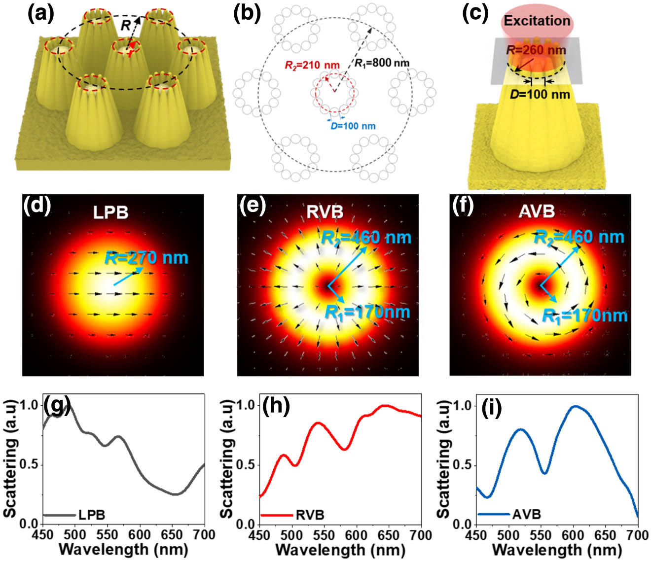
Figure 1(a) is the sketch map of one PTCC unit surrounded by six PTCC units equally spaced on a circle. The position relationship between the PTCC unit and the six PTCC units is shown in Fig. 1(b), and the radius of the PTCC unit is
![]()
Figure 1.(a) Sketch map of one PTCC unit equidistantly surrounded by six other PTCC units; (b) position relationship between one PTCC unit and the six PTCC units equally spaced on a circle; (c) structure parameters of one PTCC unit; transverse electric field component of (d) LPB, (e) RVB, and (f) AVB tightly focused via an micro-objective (MO) with NA = 0.85; scattering spectra of one PTCC unit vertically illuminated via the (g) LPB, (h) RVB, and (i) AVB in the range of 450–700 nm.
Based on the three-dimensional finite-difference time-domain (3D-FDTD, Lumerical) method[18], the scattering characteristic of one PTCC unit was simulated. Due to the multiple plasmon nanotips inside one unit, the interference between these plasmon nanotips leads to multiple resonances supported by one unit. These resonances can be excited by optimizing the coupling between the incident light and the mode field distributions of these resonances, such as illumination by the light beams (LPB, RVB, or AVB) with different electric field distributions. Based on the Richard–Wolf theory[19], the tight focusing characteristics of the LPB, RVB, and AVB are calculated. Figures 1(d)–1(f) are the transverse electric field component of the tightly focused LPB, RVB, and AVB, respectively, under focusing via a microobjective with a numerical aperture (NA) of 0.85. As shown in Fig. 1(d), the radius of the transverse electric field component of the tightly focused LPB is 270 nm. When the tightly focused LPB was illuminated on the center of one PTCC unit, it could illuminate all the plasmonic tips of the PTCC unit. The outside diameter of the PTCC unit is 260 nm, which is smaller than the radius of the transverse electric field component of the focused LPB. Figure 1(g) is the scattering spectrum of one PTCC unit in the range of 450–700 nm, under tightly focused LPB vertically illuminating the center of one PTCC unit. Note that the PTCC unit has optimized plasmon resonance in the short wavelength range.
Figure 1(h) shows the scattering spectrum of one PTCC unit under vertical illumination of the tightly focused RVB, whose transverse electric field component is shown in Fig. 1(e), with the donut-shaped intensity distribution and inner and outer diameters being 170 and 460 nm, respectively. Note that the PTCC unit has optimized plasmon resonance in the long wavelength range. Figure 1(i) is the scattering spectrum of one PTCC unit under vertical illumination of the focused AVB. The corresponding transverse electric field component is shown in Fig. 1(f), with the donut-shaped intensity distribution, and the inner and outer diameters being 170 and 460 nm, respectively. The PTCC unit has optimized plasmon resonance in the middle wavelength range. Although the mode field distributions of the tightly focused RVB and AVB are the same, the spatial electric field vectors of the two focused beams have a significant influence on the plasmon resonance of the PTCC unit. Therefore, when the nanostructure is unchanged, only by changing the spatial electric field vector of the excitation light, can the plasmon resonance characteristic of the PTCC unit be adjusted.
The electric field enhancement characteristic of the PTCC array was calculated using the 3D-FDTD method[20]. The center of one PTCC unit was illuminated via the tightly focused LPB, RVB, and AVB, as sketched in Figs. 2(a)–2(c), respectively. The arrows in Figs. 2(a)–2(c) represent the spatial electric field vectors of the three kinds of excitation light. Due to the mode field size of the tightly focused LPB (
![]()
Figure 2.(a)–(c) Sketch maps of the excitation light with three kinds of spatial electric field vectors vertically illuminating the center of one PTCC unit; (d)–(f) electric-field intensity and (g)–(i) charge distributions at the bottom of one PTCC unit when the center of one PTCC unit was illuminated via the focused LPB, RVB, and AVB, respectively.
The tightly focused RVB was focused on one PTCC unit, as sketched in Fig. 2(b). Compared with the tightly focused LPB, although the donut-shaped intensity distribution of the tightly focused RVB can irradiate most of the energy to one PTCC unit, its radial polarization is perpendicular to the center line of any two adjacent plasmonic tips. Therefore, RVB can only excite the surface localized mode on one PTCC unit, instead of the gap mode between two adjacent plasmonic tips. Figures 2(e) and 2(h) are the electric field intensity and charge distributions of the surface localized mode with
The EF of the PTCC array was further calculated when the LPB, RVB, and AVB were illuminated on the center of the two adjacent PTCC units, as shown in Fig. 3(a). Figures 3(b)–3(d) show the corresponding calculation results of the electric field intensity enhancement of the PTCC. Compared with the focused LPB irradiating the center of one PTCC unit, irradiating the center of two adjacent PTCC units not only obtains more hot spots, but also increases the electric field intensity enhancement factor
![]()
Figure 3.(a) Sketch maps of the tightly focused LPB, RVB, and AVB vertically illuminated on the center of two adjacent PTCC units; (b)–(d) electric field intensity distributions of the four PTCC units corresponding to LPB, RVB, and AVB illumination, respectively.
Figure 4(a) shows the fabrication process of the PTCC array. Based on the Langmuir–Blodgett (LB) self-assembled method[21], a monolayer-ordered hexagonally closed-packed polystyrene (PS) nanosphere with diameter of 800 nm was assembled on the surface of the silicon wafer, and then etched by ICP for 3 min, so as to construct a periodic nanocone array on the surface of the silicon wafer. Then, the periodic nanocone array was further etched for 2 min to form the silicon nanotip circular cluster arrays. Lastly, a 40 nm thick Ag film was deposited on the silicon nanotips circular cluster array via the electron beam evaporator.
![]()
Figure 4.(a) Sketch map of the fabrication process of the PTCC array; (b) SEM image of PTCC array with scale bar of 10 µm; the inset is the microimage of the PTCC array on a 2 cm silicon wafer; (c) SEM image of the PTCC array with scale bar of 800 nm; the inset is one PTCC unit with tip curvature radius of ∼20 nm; (d) measured reflection spectrum (black curve) and the calculated scattering spectrum (red curve) of the PTCC array.
The microscopy image of the PTCC array on a 2 cm silicon wafer is shown as the inset in Fig. 4(b). Figure 4(b) is a scanning electron microscope (SEM) image of the PTCC array with scale bar of 10 µm, illustrating that the PTCC array has been prepared uniformly over large areas. Figure 4(c) is the SEM image of the PTCC array with higher magnification, and the inset is one PTCC unit with a tip curvature radius of
Based on the calculated results of the electric field enhancement of the PTCC array illuminated via the LPB, RVB, and AVB, note that the electric field enhancement under LPB and AVB illumination is not very sensitive to the position of the excitation light irradiated on the PTCC array. Therefore, we only experimentally compare the enhancement of the Raman spectra intensity under the excitation of LPB and AVB. Figure 5(a) is the sketch map of the experimental configuration for SERS examination. A He–Ne laser at wavelength of 632.8 nm was adopted as the excitation source, which was focused on the PTCC array via a
![]()
Figure 5.(a) Sketch map of experimental setup for SERS examination; (b) Raman spectra of MG, with concentration from 10−10 M down to 10−13 M, absorbed on the PTCC array and excited via LPB and AVB, respectively; (c) Raman mapping of MG with concentrations of 10−8 M. The inset is the histogram of the intensities of 1587 cm−1 characteristic peak obtained along the white dashed in (c); (d) Raman spectra of MG with concentrations of 10−12 M (red curve) and 10−3 M (black curve) on PTCC and Si substrates, respectively.
The electric field enhancement of the PTCC array was further quantitatively analyzed under MG concentration of
Based on the examination results of
SERS uniformity of the PTCC array was further examined via Raman mapping[23]. Figure 5(c) is the Raman mapping result within a region of
3. Conclusion
In summary, we use AVB to illuminate the PTCC array to significantly enhance the electric near-field intensity of the PTCC array, and then use it to improve SERS sensitivity. The PTCC array was prepared based on the self-assembled and ICP etching. Simulation results show that, compared with LPB and RVB excitations, the AVB excitation can obtain the optimized electric near-field enhancement, no matter whether it is an electric field enhancement factor or a hot spot number. Experimental results proved that AVB excitation can significantly improve SERS examination sensitivity compared with LPB excitation. Meanwhile, the PTCC array had excellent uniformity with the Raman enhancement factor, calculated to be
References
[1] S. Nie, S. Emory. Probing single molecules and single nanoparticles by surface-enhanced Raman scattering. Science, 275, 1102(1997).
[2] K. Kneipp, Y. Wang, H. Kneipp, L. Perelman, I. Itzkan, R. Dasari, M. Feld. Single molecule detection using surface-enhanced Raman scattering (SERS). Phy. Rev. Lett., 78, 1667(1997).
[3] C. Haynes, A. McFarland, R. Van Duyne. Surface-enhanced Raman spectroscopy. Anal. Chem., 77, 388(2005).
[4] J. Li, Y. Huang, Y. Ding, Z. Yang, S. Li, X. Zhou, F. Fan, W. Zhang, Z. Zhou, D. Wu, B. Ren, Z. Wang, Z. Tian. Shell-isolated nanoparticle-enhanced Raman spectroscopy. Nature, 464, 392(2010).
[5] P. Zhang, S. Yang, L. Wang, J. Zhao, Z. Zhu, B. Liu, J. Zhong, X. Sun. Large-scale uniform Au nanodisk arrays fabricated via X-ray interference lithography for reproducible and sensitive SERS substrate. Nanotechnology, 25, 245301(2014).
[6] M. Liu, F. Lu, W. Zhang, L. Huang, S. Liang, D. Mao, F. Gao, T. Mei, J. Zhao. Highly efficient plasmonic nanofocusing on a metallized fiber tip with internal illumination of the radial vector mode using an acousto-optic coupling approach. Nanophotonics, 8, 921(2019).
[7] B. Luk’yanchuk, N. Zheludev, S. Maier, N. Halas, P. Nordlander, H. Giessen, C. Chong. The Fano resonance in plasmonic nanostructures and metamaterials. Nat. Mater., 9, 707(2010).
[8] J. Fan, K. Bao, C. Wu, J. Bao, R. Bardhan, N. Halas, V. Manoharan, G. Shvets, P. Nordlander, F. Capasso. Fano-like interference in self-assembled plasmonic quadrumer clusters. Nano Lett., 10, 4680(2010).
[9] Y. Zhang, F. Wen, Y. Zhen, P. Nordlander, N. Halas. Coherent Fano resonances in a plasmonic nanocluster enhance optical four-wave mixing. PNAS, 110, 9215(2013).
[10] J. Fan, C. Wu, K. Bao, J. Bao, R. Bardhan, N. Halas, V. Manoharan, P. Nordlander, G. Shvets, F. Capasso. Self-assembled plasmonic nanoparticle clusters. Science, 328, 1135(2010).
[11] J. Fan, K. Bao, L. Sun, J. Bao, V. Manoharan, P. Nordlander, F. Capasso. Plasmonic mode engineering with templated self-assembled nanoclusters. Nano Lett., 12, 5318(2012).
[12] J. Fan, Y. He, K. Bao, C. Wu, J. Bao, N. Schade, V. Manoharan, G. Shvets, P. Nordlander, D. Liu, F. Capasso. DNA-enabled self-assembly of plasmonic nanoclusters. Nano Lett., 11, 4859(2011).
[13] C. Matricardi, C. Hanske, J. Garcia-Pomar, J. Langer, A. Mihi, L. Liz-Marzán. Gold nanoparticle plasmonic superlattices as surface-enhanced Raman spectroscopy substrates. ACS Nano, 12, 8531(2018).
[14] Z. Schultz, S. Stranick, I. Levin. Advantages and artifacts of higher order modes in nanoparticle-enhanced backscattering Raman imaging. Anal. Chem., 81, 9657(2009).
[15] W. Zhang, L. Huang, K. Wei, P. Li, B. Jiang, D. Mao, F. Gao, T. Mei, G. Zhang, J. Zhao. Cylindrical vector beam generation in fiber with mode selectivity and wavelength tunability over broadband by acoustic flexural wave. Opt. Express, 24, 10376(2016).
[16] A. Ahmadivand, B. Gerislioglu, N. Pala. Azimuthally and radially excited charge transfer plasmon and Fano lineshapes in conductive sublayer-mediated nanoassemblies. J. Opt. Soc. Am. B, 34, 2052(2017).
[17] T. Deng, J. Parker, Y. Yifat, N. Shepherd, N. Scherer. Dark plasmon modes in symmetric gold nanoparticle dimers illuminated by focused cylindrical vector beams. J. Phys. Chem. C, 122, 27662(2018).
[18] C. Hsu, S. Connor, M. Tang, Y. Cui. Wafer-scale silicon nanopillars and nanocones by Langmuir–Blodgett assembly and etching. Appl. Phy. Lett., 93, 133109(2008).
[19] L. Zhang, W. Zhang, F. Lu, Z. Yang, T. Xue, M. Liu, C. Meng, P. Li, D. Mao, T. Mei, J. Zhao. Azimuthal vector beam exciting silver triangular nanoprisms for increasing the performance of surface-enhanced Raman spectroscopy. Photonics Res., 7, 1447(2019).
[20] B. Richards, E. Wolf. Electromagnetic diffraction in optical systems. II. Structure of the image field in an aplanatic system. Proc. R. Soc. London Ser. A, 253, 358(1959).
[21] W. Zhang, L. Zhang, F. Lu, D. Bai, T. Xue, C. Meng, M. Liu, D. Mao, F. Gao, T. Mei. Plasmon-enhanced nonlinear nanofocusing of gold nanoprisms driven via an ultrafast azimuthal vector beam. Nanoscale, 12, 7045(2020).
[22] Y. Yu, T. Xiao, Y. Wu, W. Li, Q. Zeng, L. Long, Z. Li. Roadmap for single-molecule surface-enhanced Raman spectroscopy. Adv. Photon., 2, 014002(2021).
[23] J. Zhao, W. Sun, W. Sun, L. Liu, X. Xia, B. Quan, A. Jin, C. Gu, J. Li. Rapid templated fabrication of large-scale, high-density metallic nanocone arrays and SERS applications. J. Mater. Chem. C, 2, 9987(2014).
[24] Y. Jin, Y. Wang, M. Chen, X. Xiao, T. Zhang, J. Wang, K. Jiang, S. Fan, Q. Li. Highly sensitive, uniform, and reproducible surface-enhanced Raman spectroscopy substrate with nanometer-scale quasi-periodic nanostructures. ACS Appl. Mater. Inter., 9, 32369(2017).


Set citation alerts for the article
Please enter your email address

© Copyright 2018-2021 | Chinese Laser Press. All Rights Reserved 沪ICP备15018463号-20