• Photonics Research
  • Vol. 9, Issue 3, 389 (2021)
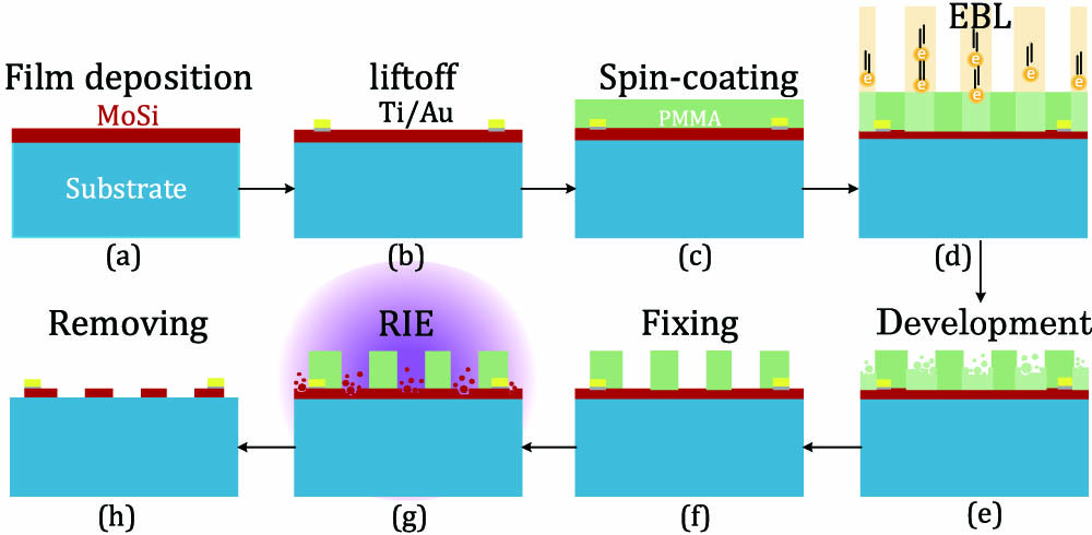
Feiyan Li1、†, Hang Han1、†, Qi Chen, Biao Zhang, Han Bao, Yue Dai, Rui Ge, Shuya Guo, Guanglong He, Yue Fei, Shuchao Yang, Xiaohan Wang, Hao Wang, Xiaoqing Jia, Qingyuan Zhao, Labao Zhang*, Lin Kang, and Peiheng Wu
Author Affiliations
  • School of Electronic Science and Engineering, Nanjing University, Nanjing 210023, China
  • show less
    DOI: 10.1364/PRJ.412697 Cite this Article Set citation alerts
    Feiyan Li, Hang Han, Qi Chen, Biao Zhang, Han Bao, Yue Dai, Rui Ge, Shuya Guo, Guanglong He, Yue Fei, Shuchao Yang, Xiaohan Wang, Hao Wang, Xiaoqing Jia, Qingyuan Zhao, Labao Zhang, Lin Kang, Peiheng Wu. Saturation efficiency for detecting 1550 nm photons with a 2 × 2 array of Mo0.8Si0.2 nanowires at 2.2 K[J]. Photonics Research, 2021, 9(3): 389 Copy Citation Text show less
    (a) Mo0.8Si0.2 film deposition on a thermally oxidized silicon wafer. (b) Fabrication of electrode pads composed of Ti and Au by lithography and liftoff. (c) Spin-coating with electron-beam resist PMMA. (d) Meandering nanowire patterning by EBL. (e) Development in methyl isobutyl ketone (MIBK) diluted in isopropanol (IPA). (f) Fixing to obtain the mask pattern. (g) Pattern transfer to the film by RIE. (h) Removal of the residual resists using N-methyl pyrrolidone.
    Fig. 1. (a) Mo0.8Si0.2 film deposition on a thermally oxidized silicon wafer. (b) Fabrication of electrode pads composed of Ti and Au by lithography and liftoff. (c) Spin-coating with electron-beam resist PMMA. (d) Meandering nanowire patterning by EBL. (e) Development in methyl isobutyl ketone (MIBK) diluted in isopropanol (IPA). (f) Fixing to obtain the mask pattern. (g) Pattern transfer to the film by RIE. (h) Removal of the residual resists using N-methyl pyrrolidone.
    (a) Comparison of the resistivity versus temperature curve of the 6.5 nm (red) and 100 nm (black) films. (b) Tcd as a function of Rs obtained by fitting the universal scaling law proposed by Ivry et al. (c) TEM image of the film, the insert shows the diffraction ring pattern. (d) The surface roughness was measured using AFM. The roughness RMS is 0.5 nm.
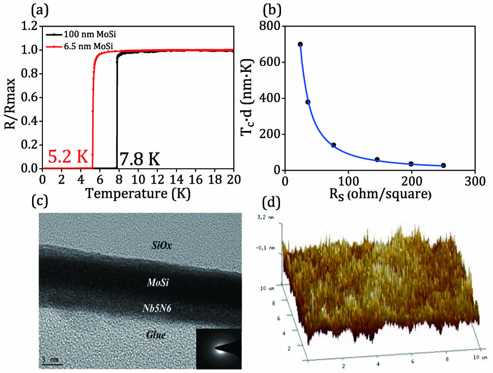
    Fig. 2. (a) Comparison of the resistivity versus temperature curve of the 6.5 nm (red) and 100 nm (black) films. (b) Tcd as a function of Rs obtained by fitting the universal scaling law proposed by Ivry et al. (c) TEM image of the film, the insert shows the diffraction ring pattern. (d) The surface roughness was measured using AFM. The roughness RMS is 0.5 nm.
    (a) Complex refractive index of the Mo0.8Si0.2 film. (b) The simulation of the optical absorption of the nanowires with different stoichiometric ratios (1550 nm wavelength).
    Fig. 3. (a) Complex refractive index of the Mo0.8Si0.2 film. (b) The simulation of the optical absorption of the nanowires with different stoichiometric ratios (1550 nm wavelength).
    Estimation of the total etching time for the Mo0.8Si0.2 film, and the optimization of the nanowires etching, representing: (1) under-etching, (2) optimum etching, (3) over-etching.
    Fig. 4. Estimation of the total etching time for the Mo0.8Si0.2 film, and the optimization of the nanowires etching, representing: (1) under-etching, (2) optimum etching, (3) over-etching.
    SEM images of the Mo0.8Si0.2 nanowires fabricated using the PMMA resist, the nanowires with a line width of 50±2 nm, a period of 200 nm, and an active area of 20 μm×20 μm.
    Fig. 5. SEM images of the Mo0.8Si0.2 nanowires fabricated using the PMMA resist, the nanowires with a line width of 50±2  nm, a period of 200 nm, and an active area of 20μm×20  μm.
    (a) I-V curves of single pixel SNSPD with 50 nm-width nanowires at different operating temperatures, ranging from 75 mK to 2.2 K. The inset figure presents ISW as a function of temperature. (b) The photon counts as functions of the bias current at different operating temperatures for the single pixel SNSPD. (c) Internal detection efficiency (IDE) and dark count rate (DCR) as functions of the normalized bias current for 50 nm-width nanowires. (d) Normalized photon counts as a function of the bias current for the 4-pixel based Mo0.8Si0.2−SNSPD at 2.2 K, the inset in the lower right corner depicts the I-V curve of one of the pixels.
    Fig. 6. (a) I-V curves of single pixel SNSPD with 50 nm-width nanowires at different operating temperatures, ranging from 75 mK to 2.2 K. The inset figure presents ISW as a function of temperature. (b) The photon counts as functions of the bias current at different operating temperatures for the single pixel SNSPD. (c) Internal detection efficiency (IDE) and dark count rate (DCR) as functions of the normalized bias current for 50 nm-width nanowires. (d) Normalized photon counts as a function of the bias current for the 4-pixel based Mo0.8Si0.2SNSPD at 2.2 K, the inset in the lower right corner depicts the I-V curve of one of the pixels.
    Film StoichiometryBulk TcnkA
    Mo0.75Si0.25 [28]7.50
    Mo0.76Si0.24 [14]7.20
    Mo0.75Si0.25 [23]7.704.702.900.55
    Mo0.83Si0.17 [24]7.605.254.770.77
    Mo0.8Si0.2 (this work)7.805.575.850.85
    Table 1. Comparison of the Different Stoichiometric Ratios of the MoSi Films in Terms of Bulk Tc, Complex Refractive Index, and FDTD Simulation Results (1550 nm Wavelength)a
    Feiyan Li, Hang Han, Qi Chen, Biao Zhang, Han Bao, Yue Dai, Rui Ge, Shuya Guo, Guanglong He, Yue Fei, Shuchao Yang, Xiaohan Wang, Hao Wang, Xiaoqing Jia, Qingyuan Zhao, Labao Zhang, Lin Kang, Peiheng Wu. Saturation efficiency for detecting 1550 nm photons with a 2 × 2 array of Mo0.8Si0.2 nanowires at 2.2 K[J]. Photonics Research, 2021, 9(3): 389
    Download Citation