Amorphous materials are attractive candidates for fabricating the superconducting nanowire single-photon detectors (SNSPDs) due to their superior tolerance and scalability over crystalline niobium nitride. However, the reduced superconducting transition temperature degenerates both operating temperature and saturation efficiency. Herein, the SNSPD (6.5 nm thickness and 50 nm width) based on the amorphous film with a high optical absorption coefficient demonstrates close-to-unity intrinsic detection efficiency for 1550 nm photons from 75 mK to 2.2 K. Further, a high-performance array SNSPD with optimized 90 nm-width wires is also demonstrated. As-fabricated uniform 4-pixel SNSPD exhibits a saturation plateau for the photon counts at 2.2 K, which overcomes the limitation of operation at low temperature () for traditional amorphous SNSPDs. Coupled with superior intrinsic quantum efficiency, highly efficient photon counts, and low dark count ratio, this detector paves a way for achieving high efficiency and superior yield for large array systems.
1. INTRODUCTION
Since the fabrication of the first superconducting nanowire single-photon detector (SNSPD) by Gol’tsman et al. [1], SNSPDs have merged as the most prevalent single-photon detectors due to their high system detection efficiency (SDE) [2], remarkably low dark count rate (DCR) [3], low timing jitter [4], ultrashort recovery time [5], and high photon count rate (PCR) [6]. Moreover, SNSPDs as advanced technologies exhibit the high potential for various applications, such as quantum optics experiments [7], quantum key distribution (QKD) for quantum communication [8], fluorescent lifetime analysis for medical applications [9], space-to-ground optical communication [10], and integrated waveguide nanophotonic circuits [11].
High internal detection efficiency (IDE) and operating temperature have always been the permanent pursuit for SNSPD; however, it is difficult to optimize the two features simultaneously [12]. The restriction stems from the internal mechanism of single photon detection by the superconducting materials. At the same time, it remains challenging for widely used NbN materials to fabricate such devices due to the crystal defects and large energy gap [13]. For this, researchers have developed novel superconductors based on amorphous materials, which have been demonstrated as promising candidates for SNSPDs [14,15]. Compared to the polycrystalline materials, the amorphous films show clear advantages in terms of tolerance and scalability. The nanowires fabricated by using amorphous materials appear to suffer from fewer constrictions, along with the high yield on the Si wafers [16]. The disordered structure offers a high degree of homogeneity and significant compatibility in the optical cavity. Moreover, the films with low energy gap are noted to be sensitive to midinfrared wavelengths [17]. Therefore, SNSPDs based on amorphous films have the potential to emerge as the desirable choice to detect the wavelengths from near-infrared to midinfrared.
According to the Bardeen–Cooper–Schrieffer relation [18], low energy gap results from low Tc, and vice versa. Based on this, the single-photon detectors fabricated from amorphous superconductors generally operate at low temperatures. For instance, the highest system detection efficiency (SDE) of 93% was achieved for the SNSPDs fabricated from amorphous WSi operated at 0.12 K at the National Institute of Standards and Technology (NIST) in 2013 [2], indicating that WSi-SNSPDs need to run below 1 K to achieve the optimal performance. In contrast, though the superconducting energy gaps of the MoSi thin films are comparable to that of WSi, their value is higher than 4 K [15]. Thus, the MoSi film becomes as a promising amorphous material for SNSPDs, which can be operated at temperature.
Sign up for Photonics Research TOC. Get the latest issue of Photonics Research delivered right to you!Sign up now
Recently, MoSi-SNSPDs have presented an excellent performance, with a detection efficiency higher than 95% at 0.7 K [19]. Besides, it has been demonstrated that a 1 μm-wide MoSi superconducting strip is capable of single-photon detection. A large active area (μμ) of the microwire single-photon detector was fabricated, which exhibited the saturated photon counts at 0.3 K [16], suggesting that the MoSi film was competent for the fabrication of SNSPD with high efficiency and large area fabrication. As mentioned above, the single-photon detectors fabricated from amorphous superconductors generally operate at low temperatures to achieve the optimal performance, which hinders their development from the fundamental research phase to the practical application.
In this study, we fabricated SNSPDs with high-performance for both high Tc and high optical absorption coefficient of films.
2. EXPERIMENT
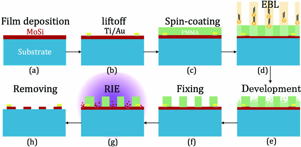
Figure 1.(a) film deposition on a thermally oxidized silicon wafer. (b) Fabrication of electrode pads composed of Ti and Au by lithography and liftoff. (c) Spin-coating with electron-beam resist PMMA. (d) Meandering nanowire patterning by EBL. (e) Development in methyl isobutyl ketone (MIBK) diluted in isopropanol (IPA). (f) Fixing to obtain the mask pattern. (g) Pattern transfer to the film by RIE. (h) Removal of the residual resists using N-methyl pyrrolidone.
In this study, the 6.5 nm-thick film has been grown on the polished and thermally oxidized silicon wafer by employing the DC magnetron sputtering from an alloy target (4-in. diameter, 1 in. = 2.54 cm) with the stoichiometry of Mo:. Before the film deposition, the sample is cleaned with Ar ion milling with the beam currents of 300 mA for 10 s and subsequently delivered to the chamber, followed by vacuum-pumping to . The sputtering process is performed at room temperature with 33 SCCM (standard cubic centimeter per minute) Ar gas, 45° throttle valve and 2 mTorr (1 Torr = 133.322 Pa) chamber pressure. Generally, the alloy target is presputtered for 5 min to clean the surface and stabilize the deposition conditions. The thickness of the film depends on the deposition rate (0.9 nm/s) and time.
Considering the poor antioxidant ability of the MoSi film, 4 nm-thick grown on the film is carried out in-situ to prevent oxidation. The film is deposited by an RF magnetron sputtering with RF power of 400 W in a 1:4 Ar and at 20 mTorr chamber pressure. Based on our previous experimental study, the chemical composition and crystalline structure of have been analyzed by using an Auger electron energy spectrometer (AES) and X-ray diffractometer (XRD). The results indicate that the sample has a Nb/N ratio of 5:6, along with a hexagonal structure [20]. Further, the film shows semiconducting electronic properties, in which the resistance rises as the temperature decreases, reaching at 4.2 K [21]. Thus, it is safe to suggest that the capping layer has no adverse impact on the superconducting film at low temperature. Simultaneously, the presence of the Nb5N6 capping layer also protects the film from degradation during the follow-up fabrication.
Figure 2.(a) Comparison of the resistivity versus temperature curve of the 6.5 nm (red) and 100 nm (black) films. (b) as a function of obtained by fitting the universal scaling law proposed by Ivry et al. (c) TEM image of the film, the insert shows the diffraction ring pattern. (d) The surface roughness was measured using AFM. The roughness RMS is 0.5 nm.
An overview of the prior work on the superconducting properties of the MoSi films has been presented in Table 1. The optimization of the film sputtering recipes to operate the devices at high temperatures has been presented. As expected, the obtained in this study is higher than the other films, allowing the detectors to operate at .
Comparison of the Different Stoichiometric Ratios of the MoSi Films in Terms of Bulk , Complex Refractive Index, and FDTD Simulation Results (1550 nm Wavelength)a
Figure 3.(a) Complex refractive index of the film. (b) The simulation of the optical absorption of the nanowires with different stoichiometric ratios (1550 nm wavelength).
Figure 4.Estimation of the total etching time for the film, and the optimization of the nanowires etching, representing: (1) under-etching, (2) optimum etching, (3) over-etching.
Figure 5.SEM images of the nanowires fabricated using the PMMA resist, the nanowires with a line width of , a period of 200 nm, and an active area of μμ.
Figure 6.(a) I-V curves of single pixel SNSPD with 50 nm-width nanowires at different operating temperatures, ranging from 75 mK to 2.2 K. The inset figure presents as a function of temperature. (b) The photon counts as functions of the bias current at different operating temperatures for the single pixel SNSPD. (c) Internal detection efficiency (IDE) and dark count rate (DCR) as functions of the normalized bias current for 50 nm-width nanowires. (d) Normalized photon counts as a function of the bias current for the 4-pixel based at 2.2 K, the inset in the lower right corner depicts the I-V curve of one of the pixels.
The photon counting measurement is carried out with continuous tunable laser at 1550 nm, and the input photon flux is attenuated by the two serial variable attenuators to a level of photons/s, calibrated with a highly precise light power meter (Thorlabs-PM100D). The SNSPDs are illuminated by using a single module fiber coupled with the input light into detector. Figure 6(b) exhibits the photon count rate (PCR) as a function of the bias current () at different operating temperatures. Notably, the device has a saturated count rate ranging from 75 mK to 2.2 K. The saturation of the PCR versus curves indicates that the detector quantum efficiency is also saturated [17]. The observed behavior suggests that the device reaches its 100% internal detection efficiency [28]. Figure 6(c) demonstrates the internal detection efficiency of the 50 nm-width SNSPD, which reveals a sigmoidal dependence on the normalized bias current, with saturation at 0.8, where the DCR value is below 1 cps. To extract the saturation level of the detector, the bias dependence of IDE is fitted with an empirical sigmoid function [29]. The red solid line in Fig. 6(c) represents the fitting curve, where the maximum IDE reaches 100%.
Notably, as a proof of the array detector, a 4-pixel array device with 90 nm-width, a period of 200 nm, and an active area of μμ has explicitly been fabricated. Figure 6(d) shows the normalized photon counts as a function of the bias current for the 4-pixel device operating at 2.2 K (inset depicting the I-V curve of one of the pixels). The is noted to be 9.5 μA with the hysteresis current of 1 μA, which is higher than the waveguide-integrated nanowire of 3.3 μA reported by Häußler [11], resulting in a higher signal-to-noise ratio. As demonstrated in the previous literature studies [28], the with a nanowire width of 110 nm and an active area of μμ exhibited saturated internal efficiency at 2.3 K. The nanowire geometric defects and constrictions are proportional to the length, and the length of the nanowires is also proportional to the active area for the same size (width and pitch) of the nanowires. Therefore, it is extremely challenging to achieve the saturated efficiency at high temperatures for large active areas. In this study, the 4-pixel array device with 90 nm-width nanowires and an active area of μμ has explicitly been fabricated, exhibiting the saturated intrinsic detection efficiency at a temperature of 2.2 K.
The I-V curves of the 4 pixels are noted to be similar for the switching current ranging from 9.0 μA to 9.5 μA. We have calculated the depairing current of SNSPD according to the equations presented by Korneeva et al. [30]. Herein, The (2.2 K) is 14.5 μA; we found the ratio of to be in the range of 0.62–0.65. This ratio supports the fact of the little constrictions during array SNSPD fabrication. Specifically, it is seen that the photon count of each pixel exhibits a saturation plateau, indicating the close-to-unity internal detection efficiency. The photon count of each pixel exhibits the maximum count rate of with dark counts at 2.2 K. Recently, the superconducting microwire was used for single photon detection with the aim of achieving saturated internal detection efficiency over a large area. The results exhibited the saturated internal detection efficiency for 1550 nm wavelengths at 0.3 K [16]. Such detectors rely on a very low temperature (mK) to achieve their excellent performance, thus, limiting the application for single photon detection. Considering that the cryogenic requirements are less complicated and less costly at 2.2 K than at , it is beneficial to have devices with optimal saturation efficiency at high temperatures, which debases the demand for the cryogenic systems and simplifies the integration of device measurement.
4. CONCLUSION
In conclusion, this work demonstrates the amorphous film exhibiting a high optical absorption coefficient in the visible to midinfrared range. The SNSPD fabricated from the film with 6.5 nm-thickness and 50 nm-width demonstrates the saturated intrinsic detection efficiency with sub 1 Hz dark count rate at a temperature of 0.2 K. Particularly, a uniform 4-pixel SNSPD has been successfully developed, exhibiting a saturation plateau for the photon counts at a temperature of 2.2 K. As a whole, the SNSPD based on films exhibits excellent advantages in operation temperature, spectral sensitivity, and internal detection efficiency.
[19] D. V. Reddy, R. R. Nerem, A. E. Lita, S. W. Nam, R. P. Mirin, V. B. Verma. Exceeding 95% system efficiency within the telecom C-band in superconducting nanowire single photon detectors. CLEO: QELS Fundamental Science, FF1A.3(2019).