• Infrared and Laser Engineering
  • Vol. 50, Issue 12, 20210424 (2021)
Lei Lv1, Dan Su1、2, Yi Yang1, Shanjiang Wang1, Huanli Zhou1, Zhaoguo Liu1, and Tong Zhang1、2、3
Author Affiliations
  • 1Joint International Research Laboratory of Information Display and Visualization, School of Electronics Science and Engineering, Southeast University, Nanjing 210096, China
  • 2Key Laboratory of Micro-Inertial Instrument and Advanced Navigation Technology, Ministry of Education, School of Instrument Science and Engineering, Southeast University, Nanjing 210096, China
  • 3Suzhou Key Laboratory of Metal Nano-Optoelectronic Technology, Southeast University Suzhou Campus, Suzhou 215123, China
  • show less
    DOI: 10.3788/IRLA20210424 Cite this Article
    Lei Lv, Dan Su, Yi Yang, Shanjiang Wang, Huanli Zhou, Zhaoguo Liu, Tong Zhang. Research progress of laser-beam-induced current microscopy technology[J]. Infrared and Laser Engineering, 2021, 50(12): 20210424 Copy Citation Text show less
    Basic model diagram of LBIC microscopy
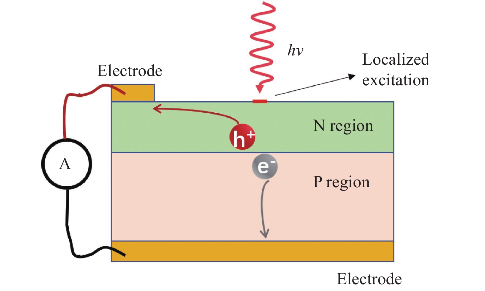
    Fig. 1. Basic model diagram of LBIC microscopy
    Classification of LBIC microscopy. (a) Excitation through microscopic objective lens; (b) Excitation through near-field fiber cone; (c) Current collection through conductive AFM probe
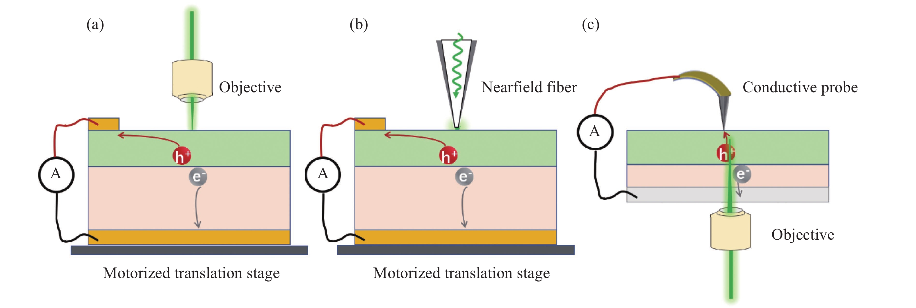
    Fig. 2. Classification of LBIC microscopy. (a) Excitation through microscopic objective lens; (b) Excitation through near-field fiber cone; (c) Current collection through conductive AFM probe
    Correlated LBIC with topography microscopic imaging technology. (a) Correlated with AFM[26]; (b) SNOM probe collects height, reflection and photocurrent at the same time[27]; (c) Correlated with SEM[24]
    Fig. 3. Correlated LBIC with topography microscopic imaging technology. (a) Correlated with AFM[26]; (b) SNOM probe collects height, reflection and photocurrent at the same time[27]; (c) Correlated with SEM[24]
    LBIC correlated with optical imaging characterization technology. (a) Absorption-LBIC correlated imaging[19]; (b) PL-LBIC correlated imaging[19]; (c) Raman-LBIC correlated imaging[30]; (d) FLIM-LBIC correlated imaging[31]
    Fig. 4. LBIC correlated with optical imaging characterization technology. (a) Absorption-LBIC correlated imaging[19]; (b) PL-LBIC correlated imaging[19]; (c) Raman-LBIC correlated imaging[30]; (d) FLIM-LBIC correlated imaging[31]
    Correlated imaging of LBIC, PL and LBIV of perovskite solar cells[35]. (a) PL imaging; (b) LBIC imaging; (c) LBIV imaging; (d) Quantitative distribution of PL intensity; (e) Quantitative distribution of PCE; (f) Overlapping of PL imaging and PCE imaging
    Fig. 5. Correlated imaging of LBIC, PL and LBIV of perovskite solar cells[35]. (a) PL imaging; (b) LBIC imaging; (c) LBIV imaging; (d) Quantitative distribution of PL intensity; (e) Quantitative distribution of PCE; (f) Overlapping of PL imaging and PCE imaging
    The influence of crystal grains and grain boundaries on device performance in CdTe photovoltaic devices[39]. (a) Absorption coefficient of CdTe; (b) Interface SEM image; (c) Surface SEM image; Microscopic LBIC imaging under different wavelength excitation (d) 532 nm, (e) 750 nm, (f) 800 nm, (g) 850 nm, (h) 880 nm, (i) 900 nm
    Fig. 6. The influence of crystal grains and grain boundaries on device performance in CdTe photovoltaic devices[39]. (a) Absorption coefficient of CdTe; (b) Interface SEM image; (c) Surface SEM image; Microscopic LBIC imaging under different wavelength excitation (d) 532 nm, (e) 750 nm, (f) 800 nm, (g) 850 nm, (h) 880 nm, (i) 900 nm
    Low-dimensional detection/photovoltaic devices. (a) Graphene devices[21]; (b) Carbon nanotube devices[42]; (c) Nanowire photovoltaic devices[3]
    Fig. 7. Low-dimensional detection/photovoltaic devices. (a) Graphene devices[21]; (b) Carbon nanotube devices[42]; (c) Nanowire photovoltaic devices[3]
    Application of micro-LBIC correlation characterization technology for the enhancement effect of bulk-material photovoltaic devices. (a) The effect of gold shell nanostructures on photocurrent of GaAs photovoltaic devices[4]; (b) NOBIC characterization of the enhancement effect of SiO2 micro-beads[44]
    Fig. 8. Application of micro-LBIC correlation characterization technology for the enhancement effect of bulk-material photovoltaic devices. (a) The effect of gold shell nanostructures on photocurrent of GaAs photovoltaic devices[4]; (b) NOBIC characterization of the enhancement effect of SiO2 micro-beads[44]
    Lei Lv, Dan Su, Yi Yang, Shanjiang Wang, Huanli Zhou, Zhaoguo Liu, Tong Zhang. Research progress of laser-beam-induced current microscopy technology[J]. Infrared and Laser Engineering, 2021, 50(12): 20210424
    Download Citation