• Photonics Research
  • Vol. 8, Issue 9, 1484 (2020)
Weihong Shen1、†, Pingyang Zeng2、†, Zelin Yang2, Di Xia2, Jiangbing Du1、*, Bin Zhang2、5, Ke Xu3, Zuyuan He1, and Zhaohui Li2、4、6
Author Affiliations
  • 1State Key Laboratory of Advanced Optical Communication Systems and Networks, Shanghai Jiao Tong University, Shanghai 200240, China
  • 2State Key Laboratory of Optoelectronic Materials and Technologies, School of Electronics and Information Technology, Sun Yat-sen University, Guangzhou 510275, China
  • 3Department of Electronic and Information Engineering, Harbin Institute of Technology (Shenzhen), Shenzhen 518055, China
  • 4Southern Marine Science and Engineering Guangdong Laboratory (Zhuhai), Zhuhai 519000, China
  • 5e-mail: zhangbin5@mail.sysu.edu.cn
  • 6e-mail: lzhh88@mail.sysu.edu.cn
  • show less
    DOI: 10.1364/PRJ.398957 Cite this Article Set citation alerts
    Weihong Shen, Pingyang Zeng, Zelin Yang, Di Xia, Jiangbing Du, Bin Zhang, Ke Xu, Zuyuan He, Zhaohui Li. Chalcogenide glass photonic integration for improved 2 μm optical interconnection[J]. Photonics Research, 2020, 8(9): 1484 Copy Citation Text show less
    (a) Cross-section sketch of the As2S3 strip waveguide showing the refractive indices of different layers. (b) Calculated effective refractive index of fundamental TE mode as a function of width and height of the strip waveguide at 1950 nm; the color area depicts the single-mode region. (c) SEM image of the cross section of strip waveguides. (d) Simulated electrical field of the fundamental TE mode in the 0.6 μm×1.2 μm strip waveguide.
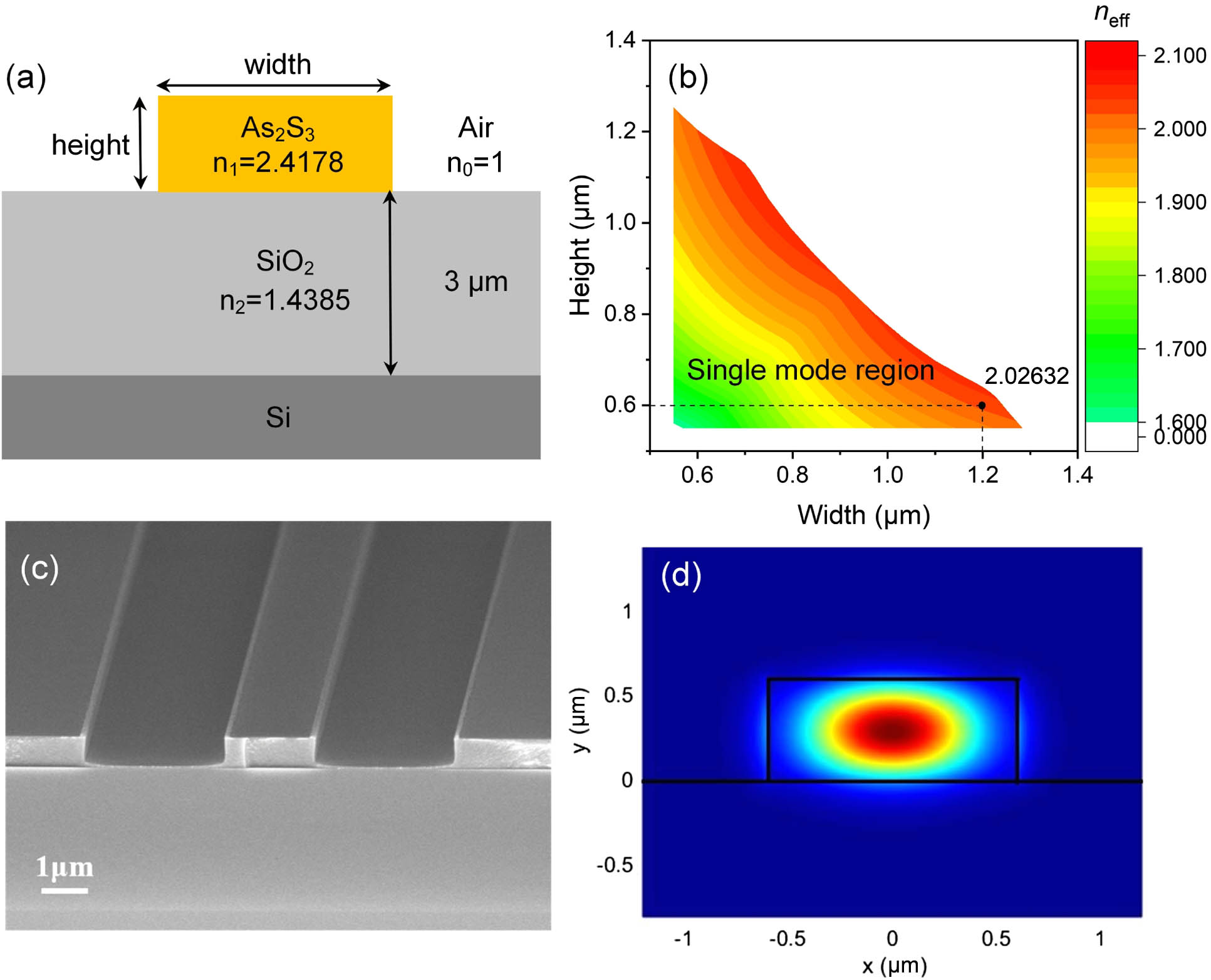
    Fig. 1. (a) Cross-section sketch of the As2S3 strip waveguide showing the refractive indices of different layers. (b) Calculated effective refractive index of fundamental TE mode as a function of width and height of the strip waveguide at 1950 nm; the color area depicts the single-mode region. (c) SEM image of the cross section of strip waveguides. (d) Simulated electrical field of the fundamental TE mode in the 0.6  μm×1.2  μm strip waveguide.
    Schematic flow of ChG fabrication process.
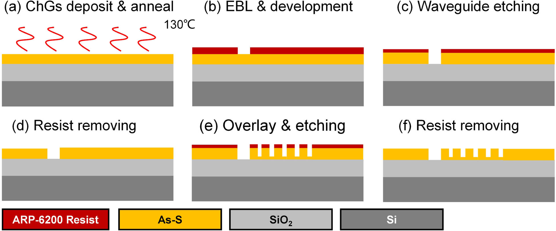
    Fig. 2. Schematic flow of ChG fabrication process.
    (a) Simulated and experimental results of the bending loss of bent waveguides versus the radius. (b) SEM image of the bent waveguides with different radii.
    Fig. 3. (a) Simulated and experimental results of the bending loss of bent waveguides versus the radius. (b) SEM image of the bent waveguides with different radii.
    (a) Measured waveguide loss and linear fitting line with the slope of 1.447 dB/cm. (b) SEM image of the spiral waveguide.
    Fig. 4. (a) Measured waveguide loss and linear fitting line with the slope of 1.447 dB/cm. (b) SEM image of the spiral waveguide.
    (a) Simulated and measured coupling efficiency of grating coupler. (b) SEM image of the fabricated grating coupler.
    Fig. 5. (a) Simulated and measured coupling efficiency of grating coupler. (b) SEM image of the fabricated grating coupler.
    (a) Simulated electrical field of mode converter for TE1 (up) and TE2 (down). (b) SEM diagram of the fabricated mode converters, inset: coupling region for phase matching. (c) Calculated coupling efficiency of mode converter for TE1 and TE2. CE, coupling efficiency; XT, crosstalk. (d)–(f) Measured transmission spectra for three modes.
    Fig. 6. (a) Simulated electrical field of mode converter for TE1 (up) and TE2 (down). (b) SEM diagram of the fabricated mode converters, inset: coupling region for phase matching. (c) Calculated coupling efficiency of mode converter for TE1 and TE2. CE, coupling efficiency; XT, crosstalk. (d)–(f) Measured transmission spectra for three modes.
    (a) Transmission spectrum of Bragg grating filters. (b) SEM diagram of fabricated Bragg gratings.
    Fig. 7. (a) Transmission spectrum of Bragg grating filters. (b) SEM diagram of fabricated Bragg gratings.
    (a) Measured insertion loss of MMIs. (b) SEM diagram of fabricated MMI.
    Fig. 8. (a) Measured insertion loss of MMIs. (b) SEM diagram of fabricated MMI.
    (a) Measured transmission spectra of MZIs. (b) SEM image of fabricated MZI.
    Fig. 9. (a) Measured transmission spectra of MZIs. (b) SEM image of fabricated MZI.
    Comparison of refractive index between SOI and As2S3 platform for C-band and 2 μm. (a) Real part of material refractive index. (b) Effective refractive index curves of strip waveguides. Symbols denote the width and corresponding neff of single-mode waveguides in the four cases.
    Fig. 10. Comparison of refractive index between SOI and As2S3 platform for C-band and 2 μm. (a) Real part of material refractive index. (b) Effective refractive index curves of strip waveguides. Symbols denote the width and corresponding neff of single-mode waveguides in the four cases.
    Comparison of devices’ performances between SOI and As2S3 platform for C-band and 2 μm. (a) Coupling spectrum of grating couplers. (b) Insertion loss of mode converters under different width deviations of fabricated waveguides.
    Fig. 11. Comparison of devices’ performances between SOI and As2S3 platform for C-band and 2 μm. (a) Coupling spectrum of grating couplers. (b) Insertion loss of mode converters under different width deviations of fabricated waveguides.
    Experiment setup of (1) 2 μm on-chip MDM interconnection and (2) As2S3 chip broadband testing. Insets show optical spectrum of (i) modulated 2 μm signal, (ii) ASE broadband source, and (iii) the on-chip three-mode multiplexing.
    Fig. 12. Experiment setup of (1) 2 μm on-chip MDM interconnection and (2) As2S3 chip broadband testing. Insets show optical spectrum of (i) modulated 2 μm signal, (ii) ASE broadband source, and (iii) the on-chip three-mode multiplexing.
    Measured BER curves of (a) 70 Gbps PAM4 and (b) 80 Gbps PAM4, under the BTB case and after 3 MDM channel transmission. Insets (i)–(iv): eye diagrams of PAM4 signals marked in (a) and (b).
    Fig. 13. Measured BER curves of (a) 70 Gbps PAM4 and (b) 80 Gbps PAM4, under the BTB case and after 3 MDM channel transmission. Insets (i)–(iv): eye diagrams of PAM4 signals marked in (a) and (b).
    GCSOI C-bandSOI 2 μmAs2S3 C-bandAs2S3 2 μm
    Height (μm)0.220.220.60.6
    Etch depth (μm)0.070.220.310.4
    Period (μm)0.610.831.13
    Duty cycle (μm)0.550.750.70.51
    1 dB/3 dB bandwidth (nm)38/63.337/64.335/59.365/112.5
    MCSOI C-bandSOI 2 μmAs2S3C-bandAs2S32 μm
    w0 (μm)0.450.60.61.2
    w1 (μm)0.911.221.252.45
    Gap (μm)0.150.150.150.15
    Length (μm)33.5232294
    1 dB deviation ofw0(nm)8192640
    Table 1. Comparison of the Wavelength and Fabrication Dependence
    Weihong Shen, Pingyang Zeng, Zelin Yang, Di Xia, Jiangbing Du, Bin Zhang, Ke Xu, Zuyuan He, Zhaohui Li. Chalcogenide glass photonic integration for improved 2 μm optical interconnection[J]. Photonics Research, 2020, 8(9): 1484
    Download Citation