Abstract
In this work, on-chip chalcogenide glass photonic integrations with several fundamental photonic building blocks are designed and fabricated based on the platform for improved 2 μm optical interconnection, achieving a broadened wavelength bandwidth and improved fabrication tolerance. A 600 nm thick strip waveguide has low propagation loss of 1.447 dB/cm at 2 μm. Broadband vertical coupling is realized by a grating coupler with 4.3 dB coupling loss. A Bragg grating filter, power splitter, Mach–Zander interferometer, and mode converter for on-chip mode division multiplexing (MDM) are also reported at 2 μm with reliable performances. Finally, a record high MDM optical interconnection capacity of at 2 μm is experimentally demonstrated based on the proposed chip, drawing promising prospects for future photonic integration and high-speed interconnection at the 2 μm waveband.1. INTRODUCTION
In recent years, the 2 μm waveband has attracted increasing research for broad applications, including optical communication, optical sensing, and even the next generation of gravitational-wave observatories [1]. Particularly, thanks to hollow-core fibers with low latency and low loss in an ultrawide bandwidth [2,3], and thulium (Tm) doped fiber amplifiers with a broad gain spectrum [4], 2 μm possesses the promising application of next-generation optical communication with ultralow latency and further higher capacity. Several 2 μm optical short-reach interconnections over hollow-core fibers have been carried out [5–7]. Meanwhile, the photonic integrated platform for 2 μm optical interconnection is also an essential field that needs to be exploited.
Until now, fabrications of mid-infrared (MIR) waveguides have been demonstrated in different platforms, including silicon-on-insulator (SOI) [8,9], germanium-on-silicon [10], silicon-on-sapphire [11], silicon nitride [12], indium phosphide [13], and chalcogenide glasses (ChGs) [14–16]. In the range near 2 μm, the majority of integrated waveguides are still fabricated on SOI. However, chalcogenide glass (ChG) materials, with broadband infrared transparency (0.8–20 μm [17]), have extremely low linear and nonlinear propagation loss at 2 μm. With a relatively higher refractive index of [18] than that of , more compact on-chip integration can be realized on ChG. Thanks to the slower slope of the refractive index, ChG components natively present a wider optical bandwidth and less sensitivity to fabrication deviations. In a word, all of the merits mentioned above make the low loss at 2 μm and high-density integration of ChG optical devices possible. Meanwhile, ChGs have lower two-photon absorption (10–14–10–12 m/W [19]) and negligible free-carrier concentration compared with silicon. Besides, a high nonlinear coefficient makes it realizable to obtain an efficient nonlinear effect at a lower pump threshold, e.g., stimulated Brillouin scattering [20]. As a result, ChG has been widely studied for on-chip all-optical signal processing, including frequency comb generation [21], supercontinuum generation [22], wavelength conversion [23], and so on. In addition, as it is easy to deposit ChG films on many substrates like conventional silicon or polymer substrates at low temperature (), ChG can be part of hybrid waveguides for 2 μm photonic integrated chips with other materials. Overall, holding various characteristics covering a wide application range, ChGs present a significant and promising integrated platform, particularly for 2 μm optical communications.
In this work, we build up the integrated platform with a 600 nm thick strip waveguide and several key passive components for 2 μm optical interconnection. The fabricated strip waveguide with single chip mode at 2 μm has low propagation loss of 1.4 dB/cm. The fiber-to-vertical coupling loss is optimized at 4.3 dB/facet with 123.6 nm 3 dB bandwidth around 2 μm. Other essential components, including Bragg grating filter, power splitter, Mach–Zehnder interferometer (MZI), and mode converter for on-chip mode division multiplexing (MDM), are also designed and fabricated at 2 μm with highly reliable performances. Finally, by means of the fabricated platform, we report a demonstration of on-chip MDM transmission at 2 μm, achieving a total bit rate of with error-free bit error rate lower than . The proposed platform shows attractive potential for future 2 μm optical interconnections.
Sign up for Photonics Research TOC. Get the latest issue of Photonics Research delivered right to you!Sign up now
2. CHG WAVEGUIDE DESIGN AND FABRICATION
As the guiding layer, the ChG thin film we proposed here has the composition of , sandwiched by substrate and air up-cladding, as depicted in Fig. 1(a). The strip waveguide structure was designed by the finite difference eigenmode solver in commercial Lumerical software. Only single mode should be guided in the waveguide so as to avoid modal dispersion during the signal propagation. Besides, the mode field should be confined as large as possible in the guiding layer, rather than escaping into the substrate, resulting in high absorption loss. We swept the width and height of a waveguide and calculated the supported modes working at 1950 nm in the waveguides with diverse sizes. As shown in Fig. 1(b), the single-mode region was sandwiched by two lines, the cut-off boundary of the fundamental mode and that of the first high-order mode. The color area represents the effective refractive index of the fundamental mode under different sizes of waveguides in the single-mode region. Higher indicates higher confinement factor of the guided mode, namely, the lower propagation loss. The optimized single-mode waveguide presents the size of (height × width) and of 2.02632. The simulated electrical field of fundamental transverse-electrical (TE) mode at 1950 nm is depicted in Fig. 1(d), and the confinement factor is 96.9%, which greatly reduces the absorption loss of cladding layer.
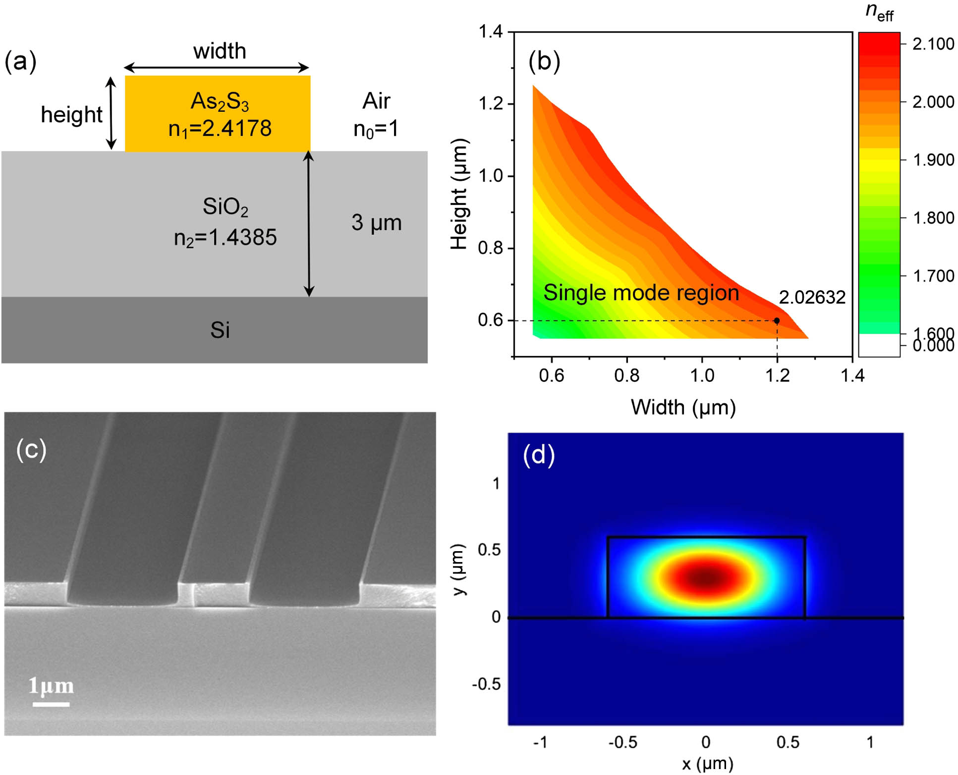
Figure 1.(a) Cross-section sketch of the strip waveguide showing the refractive indices of different layers. (b) Calculated effective refractive index of fundamental TE mode as a function of width and height of the strip waveguide at 1950 nm; the color area depicts the single-mode region. (c) SEM image of the cross section of strip waveguides. (d) Simulated electrical field of the fundamental TE mode in the strip waveguide.
The sketch of proposed fabrication process is shown in Fig. 2. The chalcogenide glass (ChG) films are deposited on the silicon substrate with a 3 μm thick thermal oxidation layer by thermal evaporation and then, going through annealing process, aims to relax the film to a stable state and improve the optical properties of the film close to bulk glass. The ChG film is purged with nitrogen, and the whole wafer is baked on a hot plate at 130°C for 5 min to form a dry and clean surface. Afterward, the electron beam photoresist ARP 6200 is spin-coated on ChG film, and the wafer is baked again on the 130°C hot plate for 5 min. Subsequently, the patterns are transferred to the photoresist by e-beam lithography. Followed by reactive ion etching, inductive coupled plasma etching, and, finally removing the resist, the strip waveguides are fabricated, as shown in Figs. 2(b)–2(d). In the case of second etching for grating structure, the patterns are mapped on each device by overlaying and etching by shallow depth using the same process mentioned before, as shown in Figs. 2(e) and 1(f).

Figure 2.Schematic flow of ChG fabrication process.
The fabricated strip waveguides are shown in Fig. 1(c) by a scanning electron microscope (SEM) image. In the chip testing setup, the 2 μm optical source is a narrow linewidth fiber laser working at 1959.34 nm. The light is coupled from fiber to on-chip waveguides by vertical coupling on the 5D alignment stage and then received by the power meter covering 2 μm. In order to measure the bending loss, 2 mm long bent waveguides with various bending radii were fabricated, as shown in Fig. 3(b). The straight waveguides with equal length near the bent ones were set as reference. The experimental results are presented as the black and red dots in Fig. 3(a). The bending loss is mainly due to the sidewall roughness, which becomes dominant as bending radius increases, and the mode mismatch between bent waveguide and straight waveguide. The measured data indicate that the waveguide bending loss with radius larger than 80 μm can be neglected, which is under 0.1 dB/mm.
Figure 3.(a) Simulated and experimental results of the bending loss of bent waveguides versus the radius. (b) SEM image of the bent waveguides with different radii.
In order to measure the waveguide propagation loss and save the device footprint at the same time, cm scale long waveguides were designed as spiral structures [24], which are shown in Fig. 4(b). Considering the minimal bending radius measured before with negligible loss, the minimum bending radius of the spiral is set as 150 μm, namely, the radius of the central curve, while that of the outer circles is greater than 300 μm. Thus, the bending loss of the spirals can be ignored approximately. The measured loss of spiral waveguides with diverse lengths is depicted in Fig. 4(a). By linear fitting, the calculated propagation loss is , which is close to the lowest loss of the integrated 2 μm waveguide proposed in Ref. [25]. Therefore, strip waveguides can support low-loss interconnection of 2 μm optical signals and maintain high integration density as well, which offers reliable backup for various functional devices.
Figure 4.(a) Measured waveguide loss and linear fitting line with the slope of 1.447 dB/cm. (b) SEM image of the spiral waveguide.
3. CHG PASSIVE DEVICES
To demonstrate the functionality of the proposed 2 μm platform, several passive devices were theoretically designed, using the finite difference time domain (FDTD) method in Lumerical, including a vertical grating coupler, Bragg grating filter, power splitter, MZI, and mode converter for on-chip mode division multiplexing (MDM). Besides, in contrast with the conventional C band and SOI platform, the wavelength dependence of the grating coupler and sensitivity to fabrication errors of the mode converter are investigated.
A. Grating Coupler
As a common device for on-chip optical coupling, the grating coupler (GC) has been developed mutually from academia to industry and is widely used due to its compact footprint and broad alignment range. The basic principle of grating diffraction is based on the Bragg’s formula, , which indicates the relationship between wavelength and grating period . Thus, the 1 dB bandwidth of coupling spectrum is generally limited at in the C-band SOI platform, which critically restricts the broadband application. While, in the proposed 2 μm platform, the optimized focused uniform GC has the calculated coupling loss of with 65 nm 1 dB bandwidth and 112.5 nm 3 dB bandwidth near 1950 nm, without any specially designed structure. The gratings were shallow-etched by 400 nm, with the period of 1.13 μm and duty cycle of 0.51. The coupling angle of fiber is optimized as ° to obtain the largest efficiency. As shown in Fig. 5(a), the fabricated GC presents the minimal coupling loss of 4.3 dB, 1 dB bandwidth of 74.2 nm, and 3 dB bandwidth of 123.6 nm (green line), which is in good accordance with the simulation results (red line). A slight blueshift of the measured coupling spectrum is owing to the shorter period of the fabricated gratings. Such a wide coupling spectrum greatly benefits the broadband wavelength division multiplexing (WDM) for on-chip 2 μm interconnection.
Figure 5.(a) Simulated and measured coupling efficiency of grating coupler. (b) SEM image of the fabricated grating coupler.
B. Mode Converter
As the most essential component for an MDM system, mode converters (MCs) have attracted much research interest in the silicon photonic platform [26]. The most common structure of MC is based on the asymmetric directional coupler (ADC) [27], in virtue of its simple design and broadband operation. ADC consists of a multimode waveguide with width and a parallel placed single-mode waveguide with width . As the phase-matching condition is satisfied, which means the of the fundamental mode in a single-mode waveguide must be equal to that of the target high-order mode in a multimode waveguide, ADC-based MC can reach the maximal coupling efficiency (CE) at certain length of coupler. Here, the optimized waveguide widths are set as and , with a 150 nm wide gap between the two waveguides. The simulated electrical fields of MCs are depicted in Fig. 6(a), with the coupling lengths of 94 and 119 μm for higher-order modes TE1 (MC1) and TE2 (MC2), respectively. From the calculated CE shown in Fig. 6(c), we can see that high CEs of and for TE1 and TE2 are obtained at 1950 nm, respectively, and the CE spectrum beyond is more than 200 nm. Besides, all the crosstalk (XT) of undesired modes is under in the span of 1850–2050 nm.
Figure 6.(a) Simulated electrical field of mode converter for TE1 (up) and TE2 (down). (b) SEM diagram of the fabricated mode converters, inset: coupling region for phase matching. (c) Calculated coupling efficiency of mode converter for TE1 and TE2. CE, coupling efficiency; XT, crosstalk. (d)–(f) Measured transmission spectra for three modes.
We employed a broadband optical source to measure the transmission spectrum of the fabricated mode converter, which has maximal 13 dBm output power and 10 dB bandwidth around 1850 nm. The ASE spectrum can be found in Section 5. The results are presented in Figs. 6(d)–6(f) for the three modes. The minimal insertion losses are 0.1, 1.22, and 1.9 dB for TE0, TE1, and TE2, respectively, with 1 dB bandwidth all beyond 80 nm. Due to the insufficient source power near 2000 nm, the crosstalk of mode converters reaches the noise floor when approaching 2000 nm, as shown in the gray areas in Figs. 6(d)–6(f). Thus, in the range from 1980 to 2020 nm, the spectrum of crosstalk climbs up gradually, which makes it fail in measuring the real crosstalk. However, according to the data at shorter wavelengths, as well as the fact that the fabricated devices show better performances at longer wavelengths, it is reasonable to suppose that the crosstalk of undesired modes is less than over the 100 nm waveband at 2 μm.
C. Filters and Splitters
In the on-chip system, filters and power splitters are basic components for optical signal processing. The filters with a central wavelength around 1950 nm are designed by Bragg gratings with the period of 476 nm and etched width of 200 nm. The SEM is shown in Fig. 7(b). Despite the measurement error, the measured period has a deviation from the designed value, which mainly results in a slight blueshift of the tested spectrum compared with the simulation results. The transmission spectrum of the Bragg gratings with diverse periods is plotted in Fig. 7(a).
Figure 7.(a) Transmission spectrum of Bragg grating filters. (b) SEM diagram of fabricated Bragg gratings.
Afterward, a multimode interferometer (MMI) based 3 dB power splitter is fabricated, with a multimode waveguide length of 15 μm and width of 5 μm, as seen in the SEM image in Fig. 8(b). After several cascaded MMIs, the measured insertion loss from one port of MMI is noted as red circles in Fig. 8(a). The fitted black line indicates the fabricated 3 dB splitter has extra insertion loss of .
Figure 8.(a) Measured insertion loss of MMIs. (b) SEM diagram of fabricated MMI.
Furthermore, based on the MMI, MZIs, which make up the basic element of modulators, are fabricated with arm length differences of 50 and 100 μm. As the measured results show in Fig. 9(a), the insertion loss ranges from 1 to 1.5 dB, and the extinction ratio is in the range of 17–23 dB from 1920 to 2020 nm. Consequently, the splitting power imbalance of MMI splitter is calculated to be 0.03. The estimated group index of the strip waveguide is about 2.7239 at 2 μm. The ripples of measured spectrum near 2000 nm are also owing to the limited bandwidth and power of broadband source.
Figure 9.(a) Measured transmission spectra of MZIs. (b) SEM image of fabricated MZI.
4. CHG’S IMPROVED WAVELENGTH AND FABRICATION DEPENDENCE
As noted, a conventionally designed GC has the coupling spectrum strongly related to wavelength, which limits the 1 dB bandwidth just about 30 nm without special design. Besides, the coupling efficiency of ADC-based MC is sensitive to the fabrication deviation of waveguide width. Generally, the width of a waveguide etched by lithography has a deviation of several tens of nanometers, which is large enough to break down the phase-matching condition, as a result of the large insertion loss of ADC. In this paper, the two problems are called the GC’s wavelength dependence and MC’s sensitivity to fabrication errors for short. In fact, one common reason for these problems comes from the refractive index as a function of wavelength and waveguide structure. In other words, the change with wavelength contributes to the coupling efficiency of GC with limited bandwidth, and, similarly, change with waveguide width also makes the coupling efficiency of MC sensitive to the fabrication deviation of waveguide width. However, such circumstances vary in different material systems.
We provide a comparison of refractive index and device performances on the conventional 220 nm thick SOI platform or 600 nm thick platform, at C-band or 2 μm, respectively. The real part of refractive index of Si relative to wavelength is depicted as a blue line in Fig. 10(a), and that of is plotted as an orange line combined by experimental data (solid line) and fitted data (dash line). Figure 10(b) shows the effective refractive index of strip waveguides in the four cases. The curve with sharper slope indicates a stronger relationship with wavelength or waveguide width. of presents a slower curve in the 1.5–2 μm range compared with that of Si, and longer wavelength in the same material platform appears as a gentler curve of . As a result, the 2 μm platform shows the least relativity between and wavelength/waveguide width, which illustrates that 2 μm devices have improved dependence on wavelength and fabrication deviation of width.
Figure 10.Comparison of refractive index between SOI and platform for C-band and 2 μm. (a) Real part of material refractive index. (b) Effective refractive index curves of strip waveguides. Symbols denote the width and corresponding of single-mode waveguides in the four cases.
Based on the four diverse platforms, we simulated the coupling efficiency of GC versus wavelength and that of MC versus deviation of waveguide width , as plotted in Figs. 11(a) and 11(b), respectively. The simulation parameters and results are listed in Table 1. The calculated 3 dB bandwidth of 2 μm GC on is 112.5 nm, which is nearly 1.8 times wider than that of C-band GC on SOI; further, 2 μm MC on presents the least dependence on fabrication deviation (red line), with the 1 dB bandwidth of 40 nm, which is four times larger than SOI MC at C-band. The measured efficiency of the fabricated MC at 2 μm is displayed in green star symbols in Fig. 11(b), with good consistence with the simulation result. Thus, these results fully confirm that components have broadened wavelength bandwidth and improved fabrication tolerance at 2 μm.
Figure 11.Comparison of devices’ performances between SOI and platform for C-band and 2 μm. (a) Coupling spectrum of grating couplers. (b) Insertion loss of mode converters under different width deviations of fabricated waveguides.
| GC | SOI C-band | SOI 2 μm | As2S3 C-band | As2S3 2 μm |
| Height (μm) | 0.22 | 0.22 | 0.6 | 0.6 |
| Etch depth (μm) | 0.07 | 0.22 | 0.31 | 0.4 |
| Period (μm) | 0.6 | 1 | 0.83 | 1.13 |
| Duty cycle (μm) | 0.55 | 0.75 | 0.7 | 0.51 |
| 1 dB/3 dB bandwidth (nm) | 38/63.3 | 37/64.3 | 35/59.3 | 65/112.5 |
| MC | SOI C-band | SOI 2 μm | As2S3C-band | As2S32 μm |
| w0 (μm) | 0.45 | 0.6 | 0.6 | 1.2 |
| w1 (μm) | 0.91 | 1.22 | 1.25 | 2.45 |
| Gap (μm) | 0.15 | 0.15 | 0.15 | 0.15 |
| Length (μm) | 33.5 | 23 | 22 | 94 |
| 1 dB deviation ofw0(nm) | 8 | 19 | 26 | 40 |
Table 1. Comparison of the Wavelength and Fabrication Dependence
5. CHG FOR 2 μm OPTICAL INTERCONNECTION
All the above fabricated devices can be applied for the on-chip optical interconnection at 2 μm, especially the mode converter for the MDM system. Here, in order to confirm the communication application of the proposed ChG chip, we demonstrate the high-speed on-chip MDM transmission at 2 μm. The system setup is shown in Fig. 12(1). The four-pulse amplitude modulation (PAM4) electrical signals were generated by the AWG with a 64 GSa/s sampling rate, amplified by the wideband electrical amplifier (EA), and then converted to optical signals via the lithium niobate Mach–Zehnder modulator (MZM) with 12 GHz bandwidth at 2 μm. The spectrum of the modulated optical signal is shown in Fig. 12(i). A thulium-doped fiber amplifier (TDFA) was previously employed to compensate for the insertion loss of the MDM chip. The fibers we used in the whole setup were standard single-mode fiber, which has insignificant propagation loss of 2 μm light in a few meters length. An optical bandpass filter after the chip eliminated the amplified spontaneous emission (ASE) noise brought by TDFA. The modulated optical signal after transmission was received by a PD with 22 GHz bandwidth and then sent into a real-time oscilloscope with a sampling rate of 160 GSa/s for the off-line digital signal processing (DSP). High-speed PAM4 signal was transmitted in the 2 μm MDM link, by means of the root raised cosine filter with a roll-off factor of 0.01 to compress the signal bandwidth. The matched filter and the time-domain feed forward equalization (FFE) were applied at the receiver side to obtain the lower bit error ratios (BERs). It needs to be noted that, the DSP settings are all the same for each channel transmission, so as to evaluate the performances fairly. Besides, the setup of broadband testing is shown in Fig. 12(2) with the ASE spectrum depicted in Fig. 12(ii).
Figure 12.Experiment setup of (1) 2 μm on-chip MDM interconnection and (2) chip broadband testing. Insets show optical spectrum of (i) modulated 2 μm signal, (ii) ASE broadband source, and (iii) the on-chip three-mode multiplexing.
In this experiment, we finally achieved on-chip MDM interconnection at 2 μm, which holds 12 times larger capacity than the results reported in Ref. [28] and breaks the record of total capacity for 2 μm optical communication. The calculated BER curves of 35 GBaud/s and 40 GBaud/s PAM4 signals are plotted in Fig. 13, and the eye diagrams of back-to-back (BTB) and three mode channels after FFE are also described. The performance at the BTB case shows a low BER of 5.47 × 10⁻⁴ for 35 GBaud/s and 1.12 × 10⁻³ for 40 GBaud/s under the received power of 5 dBm. After MDM transmission of chip, all the three mode channels present reliable BER performances under the 7% forward error correction (FEC) threshold (3.8 × 10⁻³) at the same received power. The measured power penalties of 35 GBaud/s PAM4 signals at 7% FEC threshold are 0.4, 1.1, and 1.7 dB for the TE0, TE1, and TE2 modes, respectively, and those of 40 GBaud/s signals are 1.3, 2.1, and 2.8 dB, which are mainly contributed by the insertion loss of the MDM chip. As for the lack of fiber arrays for parallel coupling, we were unable to transmit the MDM channels at the same time, while the measured modal crosstalk of less than is low enough to ignore the intermode-channel interference. Thus, the power penalty in actual MDM transmission will be slightly higher than that we measured. In addition, the TDFA we employed here becomes unstable as the gain increases to the peak value. Thus, the received power cannot be higher than 5 dBm. Besides, the total loss of the MDM chip also worsens the signal-to-noise ratio. With improved performances of TDFA and even lower coupling loss of an MDM chip, we can obtain further higher transmission speeds in the 2 μm MDM system.
Figure 13.Measured BER curves of (a) 70 Gbps PAM4 and (b) 80 Gbps PAM4, under the BTB case and after 3 MDM channel transmission. Insets (i)–(iv): eye diagrams of PAM4 signals marked in (a) and (b).
6. SUMMARY
In this paper, we have demonstrated a 2 μm photonic integrated platform based on 600 nm thick strip waveguides. The characteristics of the platform, including propagation loss and bending loss are measured, and performances of several fundamental components, such as grating coupler, mode converter, filter, and power splitter, are discussed. Compared with the conventional SOI platform, the proposed 2 μm platform presents improved wavelength dependence (wider optical bandwidth) and better tolerance of fabrication deviations. Besides, based on the fabricated MDM chip, we demonstrated the on-chip MDM interconnection at 2 μm with the highest total speed of . The results reported in this paper provide a cornerstone of the photonic integrated platform for 2 μm optical interconnection.
References
[1] F. C. G. Gunning, B. Corbett. Time to open the 2-μm window?. Opt. Photon. News, 30, 42-47(2019).
[2] H. Sakr, T. D. Bradley, Y. Hong, G. T. Jasion, J. R. Hayes, H. Kim, I. A. Davidson, E. N. Fokoua, Y. Chen, K. R. H. Bottrill, N. Taengnoi, P. Petropoulos, D. J. Richardson, F. Poletti. Ultrawide bandwidth hollow core fiber for interband short reach data transmission. Optical Fiber Communication Conference, Th4A-1(2019).
[3] T. Bradley, G. Jasion, J. Hayes, Y. Chen, L. Hooper, H. Sakr, M. A. Gouveia, A. Taranta, A. Saljoghei, H. C. Mulvad, M. Fake, I. Davidson, N. V. Wheeler, E. N. Fokoua, W. Wang, S. R. Sandoghchi, D. Richardson, F. Poletti. Antiresonant hollow core fibre with 0.65 dB/km attenuation across the C and L telecommunication bands. European Conference on Optical Communication, 1-4(2019).
[4] Z. Li, A. M. Heidt, N. Simakov, Y. Jung, J. M. O. Daniel, S. U. Alam, D. J. Richardson. Diode-pumped wideband thulium-doped fiber amplifiers for optical communications in the 1800–2050 nm window. Opt. Express, 21, 26450-26455(2013).
[5] Z. Liu, Y. Chen, Z. Li, B. Kelly, R. Phelan, J. O’Carroll, T. Bradley, J. P. Wooler, N. V. Wheeler, A. M. Heidt, T. Richter, C. Schubert, M. Becker, F. Poletti, M. N. Petrovich, S. Alam, D. J. Richardson, R. Slavík. High-capacity directly modulated optical transmitter for 2-μm spectral region. J. Lightwave Technol., 33, 1373-1379(2015).
[6] W. Shen, J. Du, C. Wang, L. Sun, K. Xu, Z. He. Single lane 90-Gbps optical interconnection at 2-μm waveband. 24th OptoElectronics and Communications Conference (OECC) and International Conference on Photonics in Switching and Computing (PSC), 1-3(2019).
[7] W. Shen, J. Du, L. Sun, C. Wang, K. Xu, B. Chen, Z. He. 100-Gbps100-m hollow-core fiber optical interconnection at 2-μm waveband by PS-DMT. Optical Fiber Communication Conference, Th2A.1(2020).
[8] S. A. Miller, M. Yu, X. Ji, A. G. Griffith, J. Cardenas, A. L. Gaeta, M. Lipson. Low-loss silicon platform for broadband mid-infrared photonics. Optica, 4, 707-712(2017).
[9] J. Li, Y. Liu, Y. Meng, K. Xu, J. Du, F. Wang, Z. He, Q. Song. 2 μm wavelength grating coupler, bent waveguide, and tunable microring on silicon photonic MPW. IEEE Photon. Technol. Lett., 30, 471-474(2018).
[10] G. Z. Mashanovich, C. J. Mitchell, J. S. Penades, A. Z. Khokhar, C. G. Littlejohns, W. Gao, Z. Qu, S. Stanković, F. Y. Gardes, T. B. Masaud, H. M. H. Chong, V. Mittal, G. S. Murugan, J. S. Wilkinson, A. C. Peacock, M. Nedeljkovic. Germanium mid-infrared photonic devices. J. Lightwave Technol., 35, 624-630(2017).
[11] Y. Zou, H. Subbaraman, S. Chakravarty, X. Xu, A. Hosseini, W.-C. Lai, P. Wray, R. T. Chen. Grating-coupled silicon-on-sapphire integrated slot waveguides operating at mid-infrared wavelengths. Opt. Lett., 39, 3070-3073(2014).
[12] J. X. B. Sia, G. T. Reed, H. Wang, W. Wang, X. Guo, J. Zhou, Z. Zhang, X. Li, Z. L. Qiao, C. Y. Liu, C. Littlejohns. SiN-SOI multilayer platform for prospective applications at 2 μm. IEEE Photon. J., 11, 6603809(2019).
[13] N. Ye, M. R. Gleeson, M. U. Sadiq, B. Roycroft, C. Robert, H. Yang, H. Zhang, P. E. Morrissey, N. M. Suibhne, K. Thomas, A. Gocalinska, E. Pelucchi, R. Phelan, B. Kelly, J. O’Carroll, F. H. Peters, F. C. G. Gunning, B. Corbett. InP-based active and passive components for communication systems at 2 μm. J. Lightwave Technol., 33, 971-975(2015).
[14] P. Ma, D. Choi, Y. Yu, Z. Yang, K. Vu, T. Nguyen, A. Mitchell, B. Luther-Davies, S. Madden. High Q factor chalcogenide ring resonators for cavity-enhanced MIR spectroscopic sensing. Opt. Express, 23, 19969-19979(2015).
[15] W. Shen, P. Zeng, J. Du, B. Zhang, Z. Li, K. Xu, Z. He. Chalcogenide photonic integration at 2-μm with improved wavelength and fabrication dependency. Conference on Lasers and Electro-Optics (CLEO), STh4L(2020).
[16] X. Gai, D. Choi, S. Madden, Z. Yang, R. Wang, B. Lutherdavies. Super-continuum generation in the mid-infrared from a dispersion-engineered As2S3 glass rib waveguide. Opt. Lett., 37, 3870-3872(2012).
[17] L. Zhang, W. Zhang, X. Wang, P. Zhang, S. Dai, Q. Nie. Investigation of Ge20Sb15Se65 photonic crystal slab waveguides with slow light at infrared wavelength. Opt. Mater. Express, 3, 1438-1443(2013).
[18] B. Eggleton, B. Luther-Davies, K. Richardson. Chalcogenide photonics. Nat. Photonics, 5, 141-148(2011).
[19] A. Zakery, S. R. Elliott. Optical properties and applications of chalcogenide glasses: a review. J. Non-Crystalline Solids, 330, 1-12(2003).
[20] R. Pant, D. Marpaung, I. V. Kabakova, B. Morrison, C. G. Poulton, B. J. Eggleton. On-chip stimulated Brillouin scattering for microwave signal processing and generation. Laser Photon. Rev., 8, 653-666(2014).
[21] M. Merklein, I. V. Kabakova, T. F. S. Buttner, D. Choi, B. Lutherdavies, S. J. Madden, B. J. Eggleton. Enhancing and inhibiting stimulated Brillouin scattering in photonic integrated circuits. Nat. Commun., 6, 6396(2015).
[22] Y. Yu, X. Gai, P. Ma, D. Choi, Z. Yang, R. Wang, S. Debbarma, S. J. Madden, B. Luther-Davies. A broadband, quasi-continuous, mid-infrared supercontinuum generated in a chalcogenide glass waveguide. Laser Photon. Rev., 8, 792-798(2014).
[23] M. Pelusi, V. G. Taeed, L. Fu, E. C. Magi, M. R. E. Lamont, S. Madden, D.-Y. Choi, D. A. P. Bulla, B. Luther-Davies, B. J. Eggleton. Applications of highly-nonlinear chalcogenide glass devices tailored for high-speed all-optical signal processing. IEEE J. Sel. Top. Quantum Electron., 14, 529-539(2008).
[24] A. D. Simard, Y. Painchaud, S. Larochelle. Integrated Bragg gratings in spiral waveguides. Opt. Express, 21, 8953-8963(2013).
[25] M. Rouifed, C. G. Littlejohns, T. X. Quo, H. Qiu, T. Hu, Z. Zhang, C. Liu, G. T. Reed, H. Wang. Low loss SOI waveguides and MMIs at the MIR wavelength of 2 μm. IEEE Photon. Technol. Lett., 28, 2827-2829(2016).
[26] Y. Liu, K. Xu, S. Wang, W. Shen, H. Xie, Y. Wang, S. Xiao, Y. Yao, J. Du, Z. He, Q. Song. Arbitrarily routed mode-division multiplexed photonic circuits for dense integration. Nat. Commun., 10, 3263(2019).
[27] D. Dai, C. Li, S. Wang, H. Wu, Y. Shi, Z. Wu, S. Gao, T. Dai, H. Yu, H. K. Tsang. 10-channel mode (de)multiplexer with dual polarizations. Laser Photon. Rev., 12, 1700109(2018).
[28] S. Zheng, M. Huang, X. Cao, L. Wang, Z. Ruan, L. Shen, J. Wang. Silicon-based four-mode division multiplexing for chip-scale optical data transmission in the 2 μm waveband. Photon. Res., 7, 1030-1035(2019).

