
Xu Wang, Feng Zhou, Siqi Yan, Yuan Yu, Jianji Dong, Xinliang Zhang, "Broadband on-chip integrator based on silicon photonic phase-shifted Bragg grating," Photonics Res. 5, 182 (2017)
- Photonics Research
- Vol. 5, Issue 3, 182 (2017)
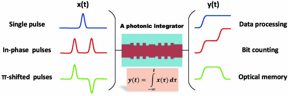
Fig. 1. Schematic of a photonic temporal integrator based on a PS-BG. Single pulse, in-phase pulses, and π-shifted pulses are integrated and used for data processing, photonic bit counting, and optical memory units, respectively.
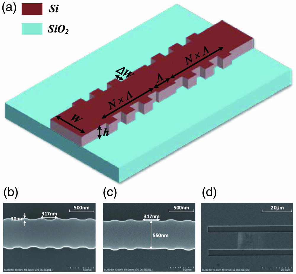
Fig. 2. (a) Schematic of the silicon PS-BG. (b) SEM image of the uniform grating. (c) SEM image of the phase-shift region. (d) SEM image of the photonic crystal coupling grating.
Fig. 3. Measured spectral response of the fabricated PS-BG with different parameters. (a) N = 200 Δ W Δ W = 20 nm N
Fig. 4. Experimental setup for optical integral. First, the optical pulse is emitted by an MLL and then reshaped by the interferometer. The interferometer has two arms for the time delay adjustment and phase adjustment. After waveform shaping, the signal is emitted into the chip and detected by the oscilloscope.
Fig. 5. (a) Normalized spectral response of the fabricated PS-BG. (b) Measured spectrum of the MLL.
Fig. 6. Experimental result of the optical integration. (a), (c), (e), (g), (i): Fitted input waveforms of the single pulse, in-phase pulses, and π-shifted pulses with different time delay (9 and 14 ps). (b), (d), (f), (h), (j): Measured (blue dots) and fitted (red line) output waveforms of the PS-BG.


Set citation alerts for the article
Please enter your email address

© Copyright 2018-2021 | Chinese Laser Press. All Rights Reserved 沪ICP备15018463号-20