Abstract
All-optical integrators are key devices for the realization of ultra-fast passive photonic networks, and, despite their broad applicability range (e.g., photonic bit counting, optical memory units, analogue computing, etc.), their realization in an integrated form is still a challenge. In this work, an all-optical integrator based on a silicon photonic phase-shifted Bragg grating is proposed and experimentally demonstrated, which shows a wide operation bandwidth of 750 GHz and integration time window of 9 ps. The integral operation for single pulse, in-phase pulses, and -shifted pulses with different delays has been successfully achieved.1. INTRODUCTION
An all-optical integrator is a device performing the time integral of an arbitrary all-optical input, which could break the speed limitation of traditional electronic devices. Due to its inherent high-speed processing ability, an all-optical integrator has been applied for data processing [1], photonic bit counting, optical memory units [2,3], and analogue computing [4].
In the optical field, the key point of an all-optical integrator is a narrow-band filter. Many schemes have been designed to realize an all-optical integrator. Some were based on the active methods, which could compensate the cavity loss and achieve a large integration time window. Asghari et al. reported a temporal integrator by cascading a discrete-time (low-speed) photonic integrator and a high-speed analog time-limited intensity integrator and experimentally achieved an integration time window of , while the bandwidth was only [5]. In 2014, a photonic temporal integrator based on an active Fabry–Perot (F–P) cavity was proposed and theoretically investigated, with an integration time window of 160 ns and an operation bandwidth of 180 GHz [6]. However, the quality () factor used in the simulation is about , which is difficult to implement experimentally. In addition, an all-optical temporal integrator based on phase-shifted distributed feedback semiconductor optical amplifier (SOA) is analyzed for the enhancement of energy transmittance and integration time window, but it is also difficult to meet the demands of the simulation conditions in real deployment [7]. Recently, a photonic temporal integrator with an InP-InGaAsP material system consisting of SOAs and current-injection phase modulators (PMs) was proposed and experimentally demonstrated [8]. An integration time window of 6331 ps with a bandwidth of 150 GHz was obtained, which showed excellent integral characteristics. Although the active methods have the potential for a large integration window, the complex control system makes it difficult to integrate on a chip.
In recent years, the passive optical network is rapidly developing, which needs massive compact and passive optical devices to support high-speed optical signal processing. A passive all-optical integrator is one of the key devices, which has been realized on fiber and silicon chip. Azaña proposed that uniform fiber Bragg grating (FBG) working in the linear regime inherently behaved as an optical temporal integrator over a limited time window in 2008, and the concepts were demonstrated by numerical simulations [9]. Later, more all-optical temporal integrators based on optical fibers were proposed and experimentally demonstrated, while the integration time window was about a few tens of picoseconds [10–12]. By cascading a time-limited ultrafast photonic temporal integrator with a discrete-time optical integrator, the integration time window of the integrator based on FBG could be expanded to 200 ps [13]. Although integrators based on FBG have been researched for a period of time and showed good performance, the drawbacks of large dimensions and the difficulty of integration with other semiconductor devices are inevitable. Silicon-based large-scale photonic integrated circuits are becoming important and promising because of the compatibility with mature complementary metal-oxide-semiconductor technologies, low cost, high stability, and ultra-compact size. In 2008, Asghari and Azaña proposed that fiber/waveguide multiple-phase-shifted Bragg grating could be used for all-optical arbitrary-order temporal integrators. The numerical simulations showed that this approach could provide optical operation bandwidths in the tens-of-GHz regime [14]. Ferrera et al. reported the first all-optical temporal integrator based on a passive microring resonator in 2010, which showed a bandwidth of 200 GHz and integration time window approaching a nanosecond [15]. After that, by reducing the factor of the microring, they enhanced the power efficiency to 1.5% and integration bandwidth exceeding 400 GHz at the cost of a short integration time window [16]. Similar to other resonating structures, the operation bandwidth of the microring is limited by the finite free spectral range (FSR). To broaden the operation bandwidth, we consider employing silicon photonic phase-shifted Bragg grating (PS-BG) as the integrator. The integrated transmission filter using a PS-BG in silicon-on-insulator (SOI) waveguides has shown a factor of within the length of 128 μm and the stopband of 10 nm [17]. The PS-BG can break the finite FSR limitation of the resonators and F–P cavity, which has the potential for high-speed optical signal processing.
Sign up for Photonics Research TOC. Get the latest issue of Photonics Research delivered right to you!Sign up now
In this paper, we propose and experimentally demonstrate an all-optical integrator based on silicon photonic PS-BG. By introducing the PS-BG as the integrator, the bandwidth limitation of the finite FSR is broken. The proposed integrator shows a wide operation bandwidth of 750 GHz and high maximum theoretical energetic efficiency of about . The integration time window of the integrator is 9 ps due to the low factor. Because of the intrinsic trade-off between bandwidth and integration time, the time-bandwidth product (defined as the ratio between the integration time window to the fastest time feature that can be accurately processed) is about 6.75, which is largely downsized with respect to the reported device. However, to the best of our knowledge, the proposed device can achieve the widest operating bandwidth among the integrators on-chip.
2. OPERATION PRINCIPLE
An all-optical integrator has the ability of photon accumulation in the time domain. As shown in Fig. 1, the integral of different input optical waveforms can bring various output waveforms and applications. More specifically, the integral operation for single pulse, in-phase pulses, and π-shifted pulses can be used for data processing, photonic bit counting, and optical memory units, respectively. An ideal integrator can be considered as a narrow bandpass filter, of which the transfer function can be written as below: where is the central frequency of the signal to be processed, and is the optical carrier frequency variable. In the time domain, the temporal impulse response of the ideal integrator must be proportional to the unit step function :
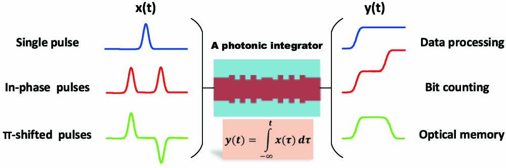
Figure 1.Schematic of a photonic temporal integrator based on a PS-BG. Single pulse, in-phase pulses, and π-shifted pulses are integrated and used for data processing, photonic bit counting, and optical memory units, respectively.
In Eq. (1), we can see the ideal integrator has infinite gain when . However, in the real world, the ideal impulse response is impossible even in the case of an active device. Therefore, a complex Lorentzian function is given for the accurate approximation to the ideal case, which corresponds to a decreasing exponential impulse response in the temporal domain as below [11]: where and are amplitude and time constants, respectively. In order to get such a transfer function, an optical resonant cavity is usually considered, such as the microring and F–P cavity. However, due to inherent FSR limitation of the resonant cavity, the operation bandwidth of the integrator is limited. There is another kind of optical filter—Bragg grating, which can realize bandpass in reflection without FSR limitation. Different from the standard Bragg filters, which show only one passband in reflection, the PS-BG has a narrow transmission peak in the stopband itself with much shorter length. Taking advantage of the high -factor peak with a broad stopband, an integrator with wide operation bandwidth can be realized.
Figure 2(a) sketches the scheme of the silicon photonic PS-BG, which has a phase-shifted region in the middle of the whole Bragg grating. The proposed structure is fabricated on a commercial SOI wafer, which consists of a 220 nm silicon layer and a 3 μm buried oxide layer. At first, the waveguide patterns are determined by electron beam lithography on the commercial SOI wafer. Next, the inductively coupled plasma etching is implemented, and the fabrication is completed. As shown in Fig. 2(b), the Bragg gratings are formed on both sidewalls of the strip waveguide. The average width of the strip waveguide, , is 550 nm. The grating width, , is 30 nm. The period of the grating is 317 nm, with the duty cycle of 50%. Figure 2(c) shows the scanning electron microscope (SEM) image of the phase-shifted region, which has the average waveguide width and length of one period. In each side of the phase-shifted region, there are 200 grating periods. Therefore, the total length of the Bragg grating is about 127 μm. Figure 2(d) shows the SEM image of the photonic crystal coupling grating, which is designed for the coupling from fiber to chip. The insertion loss is about 6 dB per facet.

Figure 2.(a) Schematic of the silicon PS-BG. (b) SEM image of the uniform grating. (c) SEM image of the phase-shift region. (d) SEM image of the photonic crystal coupling grating.
Indeed, we have chosen several groups of parameters to investigate the transmission spectrum of the PS-BG and to find the best parameters. As shown in Fig. 3(a), the three curves represent the transmission spectrum at different of 20, 30, and 40 nm. The factor and the peak transmission are (9769,0), (25,873, ), and (81,133, ), respectively. When we increase the , the coupling coefficient increases and results in higher factor with lower peak transmission. As shown in Fig 3(b), the three curves represent the transmission spectrum at of 200, 300, and 400, respectively. The factor and peak transmission are (9769, 0), (60, 819, ), and (70,988, ), respectively. We can see that, with the increase of transmission length, the reflectivity of the Bragg grating increases, which induces a higher factor and lower peak transmission. The optimal device layout for integration purposes requires both the peak transmission and the device factor to be as high as possible. As a result, we choose the group of and , which is corresponding to a factor of 25,873 and peak transmission of .
Figure 3.Measured spectral response of the fabricated PS-BG with different parameters. (a) , different of 20, 30, and 40 nm. (b) , different of 200, 300, and 400.
3. RESULTS AND DISCUSSION
The experimental setup for testing the performance of the optical integrator is shown in Fig. 4. A mode-locked laser (MLL) is used to generate Gaussian pulses, each with an FWHM of 3 ps at a repetition rate of 10 GHz. The central wavelength of the light source is adjusted to 1560.88 nm, which corresponds to the central wavelength of the integrator. The isolator (IS) is employed to avoid the light reflection, and the Er-doped fiber amplifier (EDFA) is employed to enhance the signal intensity. Then the signal is divided into two paths with orthogonal polarization by the polarization beam splitter (PBS). One path uses an optical tunable delay (OTDL) line to adjust the signal delay, and the other path uses a PM with an electrical phase shifter (EPS) to adjust the phase-shifted value between the two pulses. The two attenuators are used to balance the intensity of two pulses. After combining the two pulses by a 3 dB coupler, the signal passes through a polarization controller that fixes its polarization. By tuning the time delay and phase difference between the two pulses, we can obtain three kinds of input signal, i.e., single pulse, in-phase pulses, and -shifted pulses. The second EDFA is used to compensate the loss induced by the fiber to chip coupling. In addition, as the low energy efficiency of the passive integrator, a bandpass filter is employed to extract signals out of the background noise. At last, the waveforms are displayed and recorded on the optical oscilloscope.
Figure 4.Experimental setup for optical integral. First, the optical pulse is emitted by an MLL and then reshaped by the interferometer. The interferometer has two arms for the time delay adjustment and phase adjustment. After waveform shaping, the signal is emitted into the chip and detected by the oscilloscope.
The measured normalized spectral response of the fabricated PS-BG is shown in Fig. 5(a). The wavelength of the transmission peak is 1560.88 nm, with the 3 dB bandwidth of 0.061 nm, giving a factor of 25,588. The peak transmittance is about . As shown in Fig. 5(a), an operational bandwidth as large as (in frequency ) can be evaluated as the wavelength distance between the two consecutive minima of the transmission spectrum. The spectrum of the Gaussian pulses generated by the MLL is shown in Fig. 5(b). The overall energetic efficiency is defined by the ratio of the peak line width to the signal spectral bandwidth (both values are defined as the full width at 10% of the maximum transmission) [15]. In our device, the transmission peak line width is 21.875 GHz (0.175 nm), and signal spectral bandwidth is 379.5 GHz (3.036 nm); thus, the maximum theoretical energetic efficiency is approximately , which is higher than of the microring in Ref. [15].
Figure 5.(a) Normalized spectral response of the fabricated PS-BG. (b) Measured spectrum of the MLL.
By means of the pulse shaper based on the interferometer, we can generate different kinds of input pulses as below: (1) an ultrashort Gaussian pulse with pulse width of 3 ps [see in Fig. 6(a)]; (2) in-phase double pulses, with time delay of 9 and 14 ps [see in Figs. 6(c) and 6(g)]; (3) -shifted double pulses, with time delay of 9 and 14 ps [see in Figs. 6(e) and 6(i)].
Figure 6.Experimental result of the optical integration. (a), (c), (e), (g), (i): Fitted input waveforms of the single pulse, in-phase pulses, and π-shifted pulses with different time delay (9 and 14 ps). (b), (d), (f), (h), (j): Measured (blue dots) and fitted (red line) output waveforms of the PS-BG.
The output waveform of the single-pulsed experiment is shown in Fig. 6(b). The blue dots represent the experiment’s data, and the red dashed line represents the fitted result employing the convolution between the input pulse and in Eq. (4). When equals 23 ps, the fitted temporal impulse response could have a maximum matching to the measured result. We estimate an integration time window of 9 ps, which is defined as the time gap between 80% of the maximum integration value. The output waveforms of the in-phase double-pulsed experiment are shown in Figs. 6(d) and 6(h). Because the two pulses have the same phase, the integration results are a simple sum up of the two. The measured results show good agreement with the fitted curves both with a time delay of 9 and 14 ps. When the input pulses are -shifted, the second pulse will compensate the first pulse integration and bring a rapid decrease of the output. The output waveforms of the -shifted double-pulsed experiment are shown in Figs. 6(f) and 6(j). We can see the integration is performed without long-tailed distribution in the -shifted double-pulsed experiment.
In addition, the in-phase pulses and -shifted pulses response can be applied for photonic bit counting and optical memory units. In all three experiments, we observe good agreement between the measured integral waveforms and the ideal ones.
4. CONCLUSION
To summarize, a broadband on-chip integrator based on silicon photonic PS-BG is proposed and studied. By using a compact PS-BG with the length of 128 μm, the integrator can achieve a wide bandwidth of 750 GHz and energy efficiency of . However, because the factor of the selected PS-BG is not very high, the integration time window is 9 ps. In the passive integrator, the energy efficiency and integration time window is a trade-off and decided by the factor. In addition, the PS-BG break the FSR limitation of the microring and is promising in THz optical signal processing through the optimization design.
References
[1] D. Cotter, R. J. Manning, K. J. Blow, A. D. Ellis, A. E. Kelly, D. Nesset, I. D. Phillips, A. J. Poustie, D. C. Rogers. Nonlinear optics for high-speed digital information processing. Science, 286, 1523-1528(1999).
[2] M. T. Hill, H. J. S. Dorren, T. de Vries, X. J. M. Leijtens, J. H. den Besten, B. Smalbrugge, Y.-S. Oei, H. Binsma, G.-D. Khoe, M. K. Smit. A fast low-power optical memory based on coupled micro-ring lasers. Nature, 432, 206-209(2004).
[3] Y. Ding, X. Zhang, X. Zhang, D. Huang. Active microring optical integrator associated with electroabsorption modulators for high speed low light power loadable and erasable optical memory unit. Opt. Express, 17, 12835-12848(2009).
[4] R. Slavík, Y. Park, N. Ayotte, S. Doucet, T.-J. Ahn, S. LaRochelle, J. Azaña. Photonic temporal integrator for all-optical computing. Opt. Express, 16, 18202-18214(2008).
[5] M. H. Asghari, Y. Park, J. Azaña. Photonic temporal integration of broadband intensity waveforms over long operation time windows. Opt. Lett., 36, 3557-3559(2011).
[6] N. Huang, M. Li, R. Ashrafi, L. Wang, X. Wang, J. Azaña, N. Zhu. Active Fabry–Perot cavity for photonic temporal integrator with ultra-long operation time window. Opt. Express, 22, 3105-3116(2014).
[7] X.-H. Jia, X.-L. Ji, C. Xu, Z.-N. Wang, W.-L. Zhang. Analysis of all-optical temporal integrator employing phased-shifted DFB-SOA. Opt. Express, 22, 28530-28536(2014).
[8] W. Liu, M. Li, R. S. Guzzon, E. J. Norberg, J. S. Parker, L. A. Coldren, J. Yao. A photonic temporal integrator with an ultra-long integration time window based on an InP-InGaAsP integrated ring resonator. J. Lightwave Technol., 32, 3654-3659(2014).
[9] J. Azaña. Proposal of a uniform fiber Bragg grating as an ultrafast all-optical integrator. Opt. Lett., 33, 4-6(2008).
[10] Y. Park, T.-J. Ahn, Y. Dai, J. Yao, J. Azaña. All-optical temporal integration of ultrafast pulse waveforms. Opt. Express, 16, 17817-17825(2008).
[11] M. A. Preciado, M. A. Muriel. Ultrafast all-optical integrator based on a fiber Bragg grating: proposal and design. Opt. Lett., 33, 1348-1350(2008).
[12] M. H. Asghari, C. Wang, J. Yao, J. Azaña. High-order passive photonic temporal integrators. Opt. Lett., 35, 1191-1193(2010).
[13] M. H. Asghari, Y. Park, J. Azaña. New design for photonic temporal integration with combined high processing speed and long operation time window. Opt. Express, 19, 425-435(2011).
[14] M. H. Asghari, J. Azaña. Design of all-optical high-order temporal integrators based on multiple-phase-shifted Bragg gratings. Opt. Express, 16, 11459-11469(2008).
[15] M. Ferrera, Y. Park, L. Razzari, B. E. Little, S. T. Chu, R. Morandotti, D. J. Moss, J. Azaña. On-chip CMOS-compatible all-optical integrator. Nat. Commun., 1, 1-5(2010).
[16] M. Ferrera, Y. Park, L. Razzari, B. E. Little, S. T. Chu, R. Morandotti, D. J. Moss, J. Azaña. All-optical 1st and 2nd order integration on a chip. Opt. Express, 19, 23153-23161(2011).
[17] X. Wang, W. Shi, S. Grist, H. Yun, N. A. F. Jaeger, L. Chrostowski. Narrow-band transmission filter using phase-shifted Bragg gratings in SOI waveguide. IEEE Photonic Society 24th Annual Meeting, 869-870(2011).


