
Zhe Zhuang, Daisuke Iida, Martin Velazquez-Rizo, Kazuhiro Ohkawa. 630-nm red InGaN micro-light-emitting diodes (<20 μm × 20 μm) exceeding 1 mW/mm2 for full-color micro-displays[J]. Photonics Research, 2021, 9(9): 1796
- Photonics Research
- Vol. 9, Issue 9, 1796 (2021)
Abstract
1. INTRODUCTION
Micro-light-emitting diodes (μLEDs) have been regarded as the most promising technique for the next-generation displays due to their fast response, long lifetime, high brightness level, and low energy consumption [1–4]. The red/green/blue (RGB) μLED arrays are the basic components for full-color μLED displays. Because indium gallium nitride (InGaN)-based violet and blue LEDs have achieved great success in the past two decades, the combination of color converters and violet/blue pumping μLEDs has been considered as a feasible approach to realize RGB μLED displays [5–7]. This color-converted approach can easily integrate RGB arrays into the same substrate and obtain a wide color gamut (78%–88%) in the color space due to narrow emission spectral widths. However, the color conversion efficiency and the stability of the color converters must be improved [7–9]. When the μLED size goes below 10 μm, the luminescence uniformity and pixel patterning of the color converters become challenging.
Another promising method for full-color micro-displays utilizes RGB individual μLED chips. By integrating RGB monochromatic μLEDs from different wafers through mass-transfer process, the brightness of each pixel can be precisely controlled in a wide dynamic range, especially for high-resolution displays using ultra-small μLEDs (). In this regard, InGaN blue and green μLEDs have demonstrated remarkable performance even when the dimension shrinks down to 1 μm [10]. For the red LEDs, the aluminum indium gallium phosphide (AlInGaP) material system is generally preferred because of the outstanding efficiencies of AlInGaP red LEDs at long emission wavelengths above 600 nm [11]. However, the AlInGaP material typically has high surface recombination velocities and longer carrier diffusion lengths [12]. These characteristics lead to a significant size-dependent efficiency reduction of the AlInGaP μLEDs [13–15]. Moreover, the different absorption coefficients of InGaN and AlInGaP materials cause their μLEDs to exhibit mismatched far-field radiation patterns, resulting in the unfavorable color shift of RGB μLED displays [16]. Therefore, interest in the InGaN material system in red μLEDs has been growing.
Despite the good technological maturity of InGaN blue and green LEDs, red InGaN LEDs still suffer from a significant reduction in external quantum efficiency (EQE) when In contents increase in the InGaN active region [17,18]. The major challenge is the poor crystal quality of high-In-content InGaN quantum wells (QWs), which are caused by low-growth temperatures and large lattice mismatches between the active region and base layers. Our group developed a micro-flow method to yield high-temperature growth of InGaN layers [19,20]. To reduce the lattice mismatch, we proposed strain engineering strategies, such as utilizing substrate [21], adjusting the thickness of the GaN template [22], and optimizing the active region structures [23,24]. Other groups also put forth great effort to achieve InGaN red emission using other possible substrates, for example, InGaN red LEDs () on silicon (Si) [25], semipolar GaN substrates or templates [26,27], and InGaN platelets [28].
Sign up for Photonics Research TOC. Get the latest issue of Photonics Research delivered right to you!Sign up now
Plessey developed the red InGaN μLEDs on Si at a wavelength of 630 nm at [29]. Porotech announced the launch of its first red InGaN μLEDs at a wavelength of 640 nm at using porous GaN [30]. Another ultrasmall () red InGaN μLED using porous GaN pseudo-substrates was demonstrated with a useful on-wafer EQE of 0.2%, which was the first EQE report of red μLEDs for both AlInGaP and InGaN material systems [31]. Besides, partly relaxed InGaN pseudo-substrates were fabricated for red InGaN μLEDs, which exhibited an on-wafer EQE of 0.03% at a wavelength of 630 nm at [32]. Our group also developed μLEDs at a wavelength of 626 nm with an on-wafer EQE of 0.36% at , which was 1.8 times higher than in the previous report [33].
However, these InGaN μLEDs could have red emission () when operated at the low current density of or below. At high current densities, the emission of these μLEDs would shift to orange and amber regions due to the large blueshift of the peak wavelength. However, with some applications, such as augmented reality (AR) head-mounted displays and μLED image sources in projection systems, μLEDs operating at high current densities are required for ultrahigh brightness. Besides, the optogenetic stimulation of Chrimson by μLEDs also was shown to require a minimal optical power density of [34]. Therefore, developing InGaN red μLEDs () operated at high current densities () is crucial for satisfying ultrahigh brightness applications.
In this work, we demonstrated red InGaN μLED arrays with a peak wavelength at the current density from 10 to . We examined the high-In-content InGaN active region and the μLED structures, especially the crystal quality of nitride semiconductor sidewall interfaces. A current-voltage () curve was used to estimate the electrical performance of red μLED arrays. We also investigated the electroluminescence (EL) characteristics of red μLED arrays, including the EL peak wavelength, full-width at half maximum (FWHM), on-wafer light output power, and EQE. Finally, we utilized RGB InGaN μLED arrays to realize a wide color gamut, which covered 81.3% and 79.1% of the Rec. 2020 color spaces in CIE 1931 and 1976 diagrams, respectively.
2. EXPERIMENTAL DETAILS
The InGaN red LED epitaxial wafers were grown on -plane-patterned sapphire substrates using metal organic vapor phase epitaxy (MOVPE) in a single-wafer horizontal reactor at 100 kPa. The Ga, Al, In, and N sources were trimethylgallium (TMGa), trimethylaluminum (TMAl), trimethylindium (TMIn), and ammonia (), respectively. The precursors for n- and p-type dopings were -diluted silane and bis(cyclopentadienyl)magnesium (), respectively. High-purity , , or their mixtures were used as the carrier gases during MOVPE growth.
Indium tin oxide (ITO) was first deposited as a transparent conductive layer and underwent a subsequent two-step annealing process to form ohmic contacts with p-GaN [35]. A layer was deposited by plasma-enhanced chemical vapor deposition (PECVD) on the ITO layer to serve as a hard mask for dry etching. μLED mesas () in a array were then patterned by standard photolithography. Three inductively coupled plasma (ICP) etching processes were performed to etch through the and ITO layers and InGaN active region to expose the n-type layer. To remove the ICP-induced sidewall damage, we carried out tetramethylammonium hydroxide (TMAH) wet-etching for 40 min at room temperature. We demonstrated that this chemical treatment could improve the EQE of green μLEDs, whose peak EQE decreased by around 10% after the chemical treatment when the dimension shrank from to . The hard mask was then removed using a buffered oxide etchant [mixture of ammonium fluoride and hydrofluoric acid ( and HF)] solution, and another isolated layer was deposited by plasma-enhanced chemical vapor deposition (PECVD) for sidewall passivation [36]. Finally, we fabricated windows on the ITO and n-type layers via ICP etching and deposited Cr/Pt/Au as the n- and p-type contact pads. The trenches between mesas in the array were also covered by chromium/platinum/gold (Cr/Pt/Au) to connect every single μLED. Commercial InGaN blue and green LED wafers were used to fabricate μLED arrays as well.
The cross sections of red InGaN LED epitaxial structures and μLEDs were examined by scanning transmission electron microscopy (STEM) and high-resolution transmission electron microscopy (HRTEM). The distributions of In, Ga, and Al atoms in the epitaxial structures were measured by the energy-dispersive X-ray spectroscopy (EDS) installed in the STEM. The surface morphology of μLED arrays was observed using scanning electron microscopy (SEM). Electrical pumping of μLED arrays was implemented at the probe station using a semiconductor parameter analyzer. An integrating sphere was located above the devices to collect the on-wafer light output power for EL measurements obtained with an ultraviolet/visible (UV-vis) spectrometer. All measurements were carried out at room temperature.
3. RESULTS AND DISCUSSION
A. Structures of InGaN Red LED Wafer and μLED Devices
Figure 1(a) shows the cross-sectional STEM image of our InGaN red LED structures. Fifteen pairs of InGaN/GaN superlattices (SLs) were grown underneath the InGaN active region. The thicknesses of InGaN and GaN in the SLs were 2.4 and 5.9 nm, respectively. The InGaN active region comprised one 2.4 nm single blue QW and two 2.7 nm red QWs. The multiple barrier layers of AlN/GaN/AlGaN/GaN with the total thickness of 24 nm were utilized for strain compensation. The InGaN QWs and SLs showed a sharp contrast with barrier layers, indicating the high interface quality of the structures.
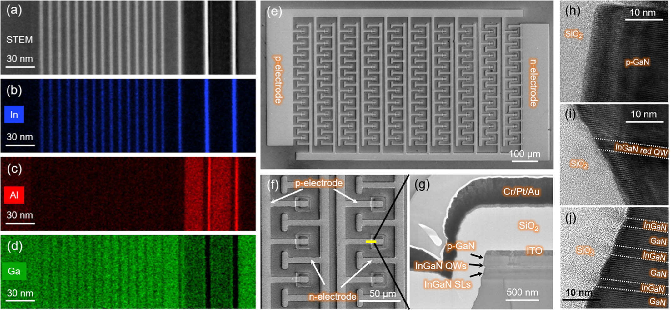
Figure 1.(a) Cross-sectional scanning transmission electron microscopy (STEM) image of our InGaN red LED structures. (b)–(d) Energy-dispersive X-ray spectroscopy (EDS) elemental mappings of In, Al, and Ga atoms distributed in the InGaN QWs and SLs using STEM EDS measurements. (e) Top-view and (f) high-resolution scanning electron microscopy (SEM) images for the red μLED array. (g) Cross-sectional TEM image of the single μLED device. (h)–(j) Cross-sectional high-resolution TEM (HRTEM) images for the interfaces between nitride materials and
The EDS elemental mappings in Figs. 1(b)–1(d) show the distribution of In, Al, and Ga atoms in our epitaxial structures. These elemental mappings offered evidence of good composition uniformity for each epitaxial layer. Besides, the Al content was higher in the thin capping layer of the InGaN red QW, but it was lower in the barrier layer. This different distribution of Al contents agreed well with our designed growth procedures, although figuring out each growth layer (AlN/GaN/AlGaN/GaN) was quite difficult because of the measurement resolution. The introduction of Al atoms in the capping and barrier layers was demonstrated to be useful for strain compensation and avoid In evaporation during the high-temperature growth of barriers [23].
Figures 1(e) and 1(f) show the top-view SEM images of the InGaN red μLED and the selected μLED arrays at a higher magnification, respectively. The n- and p-type electrodes were extended to each single μLED to guarantee uniform current injection for all μLEDs. We also measured the cross-sectional structures of the single μLED along the yellow line, as shown in Fig. 1(g). The cross-sectional TEM image in Fig. 1(g) shows that the sidewall of the InGaN μLED was passivated by a 450 nm layer. This layer also served as an isolated layer between the p-electrode and n-type nitride layers.
Generally, the sidewalls of μLEDs, especially those with the dimensions , will suffer from plasma damage during mesa-etching because energetic ion bombardment during dry-etching can induce physical damage to the plasma-exposed surfaces. This physical damage would reduce the EQE of the InGaN μLEDs [10]. TMAH or KOH wet-etching was demonstrated to be a good way to remove this physical damage [37]. We investigated HRTEM analysis of the surface regions for μLED sidewalls to examine crystal quality of the nitride semiconductors. Figures 1(h)–1(j) show the HRTEM images of the sidewall interface between nitride semiconductors and passivation layer. We observed three positions at the sidewall interface: (1) p-GaN; (2) InGaN active region; and (3) InGaN SLs. Clearly, the single crystalline atomic arrangement could be observed at the interface of these nitride sidewalls. This atomic lattice morphology demonstrated that the sidewalls of our μLEDs after chemical treatment did not show any vestiges of crystal damage [15].
B. Optoelectronic Properties of InGaN Red μLED Arrays
We investigated the absolute curve of a typical μLED array, as shown in Fig. 2(a). The corresponding absolute current density was also calculated and plotted as the right axis. Both absolute current and current density were plotted on a logarithmic scale. At the forward voltage, the curve exhibited two linear parts in the semi-logarithmic scale, which was similar to that exhibited by the single μLED chips. The transition point of the two parts, which was regarded as the turn-on voltage, was around 2.0 V. At the reverse voltage, the reversed leakage current started to increase at and reached around () at , which was a similar leakage level to that described in the other works [31]. We attributed this leakage current to many defects/dislocations generated in high-In-content QWs.
![]()
Figure 2.(a) Absolute current and current densities of a typical
Figure 2(b) shows the typical EL spectra of the μLED array at 10 and . A shoulder peak from the EL spectra was observed at around 615 nm at the low current density of . However, this shoulder peak disappeared at the higher current density of . A single-peak EL spectrum could be obtained with the peak wavelength at 630 nm and the FWHM of 62.9 nm. We presumed that the shoulder peak was regarded as the emission from the localized states [33], which originated from the In phase separation in high-In-content QWs.
The current density dependence of the peak wavelength and FWHM for the μLED array was investigated from 10 to , as shown in Fig. 2(c). We discovered that the peak wavelength of the μLED array exhibited a large blueshift of 32 nm after increasing the current density. This large blueshift value of the peak wavelength was similar to other InGaN red μLEDs [6,31], which mainly resulted from the strong quantum-confined Stark effect (QCSE) and band-filling effect in red InGaN QWs. At a current density , the FWHM of the μLED array was broad because of the localized state emission, as shown in Fig. 2(b). These localized states would be saturated at high current densities so that the FWHM continued to decrease with the increasing current density. Because the wavelength of the Rec. 2020 red primary color is 630 nm, we chose red InGaN μLEDs with a peak wavelength above 620 nm for comparison, as shown in Fig. 2(d). Achieving similar wavelengths at higher current densities was challenging because the active region required higher In contents. This work achieved red emission at much higher current densities than others [Fig. 2(d)], thus demonstrating the possibility of red InGaN μLEDs operating at high current densities.
The on-wafer EQEs of the μLED array at different current densities were measured by the integrating sphere above the sample. As shown in Fig. 2(e), the on-wafer EQE first increased rapidly with the current density and then slowly at above . This behavior was similar to the previous InGaN red μLEDs on InGaN pseudo-substrates [32], but they did not provide an explanation for this behavior. In this study, we attributed this behavior to two possible reasons. First, the relatively large leakage current in Fig. 2(a) might lead to weak emission intensity and low EQE of the μLEDs at low current densities [38]. The second dominant reason was that the high nonradiative recombination suppressed the radiative recombination [39], whose rate remained low due to the strong QCSE in high-In-content InGaN QWs. Thus, the radiative recombination was never dominant at , causing the EQE to remain low and lack an EQE peak in blue/green InGaN μLEDs. Both leakage current and nonradiative recombination are related to the dislocation density, which was regarded as the main obstacle for InGaN red μLEDs.
The on-wafer EQE reached 0.18% at a peak wavelength of 630 nm at . Previously, we estimated the EQE ratio of green (amber) μLEDs between the on-wafer measurement and absolute output measurement in the integrating sphere (μLEDs were not encapsulated with resin when measured in the integrating sphere) [33,40]. This EQE ratio was regarded as the calculated factor for the on-wafer measurement and the measurement in the integrating sphere. By multiplying the on-wafer EQE by the calculated factor, we expected an absolute EQE of 0.31%–0.47% for our red InGaN μLED array if performing measurement in the integrating sphere. This estimated EQE value is still much lower than that of blue and green InGaN μLEDs [10] and requires further improvements.
The on-wafer light output power of the μLED array reached 51 μW at [Fig. 2(e)]. The output power density (output power from unit μLED emission or mesa area) was calculated as , which was an important parameter for evaluating μLED brightness. We plotted the reported output power density values of red InGaN μLEDs in Fig. 2(f). The normal red InGaN LEDs with large chip sizes (hollow dots, absolute output power in the integrating sphere) and red AlInGaP μLEDs with similar chip sizes (on-wafer testing) are also displayed in Fig. 2(f) for comparison. The output power density in this work was the highest compared with other red InGaN μLEDs. If we estimated the absolute output power density (as with EQE estimation) in the integrating sphere (hollow red triangle with error bars), we found that the expected result in this work was comparable to normal red InGaN LEDs. Our results illustrated that the output performance of InGaN red μLEDs would not degrade significantly with the dimensions shrinking below , similar to blue InGaN μLEDs [41].
Furthermore, the output power density of AlInGaP red μLEDs at was approximately in Fig. 2(f) (measured by on-wafer testing with substrates) [14]. The AlInGaP red μLEDs had similar peak wavelengths at 632 nm. The output power from AlInGaP red μLEDs () was expected to be enhanced by 50% in maximum after removing the substrate [42]. Therefore, Fig. 2(f) indicates that our red InGaN μLEDs might have a higher output power density than the AlInGaP red μLEDs () without substrates. This comparison illustrated that the InGaN materials had great potential for high-brightness red μLEDs with the dimensions below .
C. InGaN RGB Monochromatic μLED Arrays
Finally, we fabricated InGaN blue and green μLED arrays using the same processes. The emission images of InGaN blue, green, and red μLED arrays at are shown in Fig. 3(a)–3(c), respectively. The good current spreading using n- and p-electrodes guaranteed that all of the single μLEDs in the array had the same current injection conditions and performed uniform emission under operation. These emission images definitely demonstrated the potential of the InGaN material system for RGB μLED displays.
![]()
Figure 3.(a)–(c) EL emission images of blue, green, and red
The CIE coordinates related to the emission of μLEDs are important parameters for micro-displays because they determined the physiologically perceived colors in human color vision. We calculated the coordinates of RGB μLED arrays at 20 and in both CIE 1931 and 1976 diagrams, as shown in Figs. 3(d) and 3(e), respectively. The three primary colors defined in Rec. 2020 are also displayed in Figs. 3(d) and 3(e) for comparison.
In CIE 1931 diagram, the blue μLED array had almost identical coordinates, while the green and red μLED arrays showed a small shift at . The green μLED moved away from the primary green color in Rec. 2020, while red μLED moved closed to the primary red color in Rec. 2020. Generally, the blueshift of the peak wavelength for μLEDs at high current densities should cause the coordinates to move counterclockwise, such as seen in green μLEDs [33]. The abnormal movement for the red μLED array was due to narrowing of the FWHM, which also played an important role in determining the CIE coordinates [43]. Besides, we emphasized that the coordinates of the red μLED array did not change a lot when the current density increased, which was mainly due to a peak wavelength even at (the primary red color in Rec. 2020 is at 630 nm). In the CIE 1976 diagram, the difference in the phenomenon was the lack of obvious coordinate shift in the green μLED array, which behaved in a similar manner as the blue μLED array.
We calculated the overlap of the color gamuts determined by InGaN RGB μLED arrays and Rec. 2020. At , the color gamut (dashed line triangle) by InGaN RGB μLED arrays could cover 81.5% and 76.2% of the Rec. 2020 color space in CIE 1931 and 1976 diagrams, respectively. At , the overlaps of the Rec. 2020 color space in CIE 1931 and 1976 diagrams were 81.3% and 79.1%, respectively. The overlapping results were comparable with those μLED displays using color-conversed quantum dots [5–7]. Besides, if we choose blue InGaN μLEDs closer to the primary blue color in Rec. 2020 (which has already been commercialized), higher overlap of the color space by InGaN RGB μLEDs was expected.
4. CONCLUSION
In conclusion, we demonstrated red InGaN μLED arrays that comprise every single μLED in the dimension of . The peak wavelength () emission for red InGaN μLEDs was realized at high current densities up to . Based on the on-wafer testing results, we obtained the μLEDs with a peak wavelength of 630 nm and a high light output power density of at , which is even estimated to be higher than AlInGaP red μLEDs (). The on-wafer EQE increased with the current density and reached 0.18% at . We presumed that the continuous increasing behavior of the on-wafer EQE originated from the leakage currents of the μLEDs and dominant nonradiative recombination for red InGaN QWs at low current densities. Finally, we achieved uniform luminescence of InGaN RGB μLED arrays. The color gamut determined by RGB InGaN μLED arrays covered 81.3% and 79.1% of the Rec. 2020 color space in CIE 1931 and 1976 diagrams, respectively.
Acknowledgment
Acknowledgment. The fabrication processes in this work were supported by Nanofabrication Core Labs in KAUST.
References
[1] Z. Y. Fan, J. Y. Lin, H. X. Jiang. III-nitride micro-emitter arrays: development and applications. J. Phys. D, 41, 094001(2008).
[2] K. Ding, V. Avrutin, N. Izyumskaya, U. Ozgur, H. Morkoc. Micro-LEDs, a manufacturability perspective. Appl. Sci., 9, 1206(2019).
[3] M. S. Wong, S. Nakamura, S. P. DenBaars. Review—progress in high performance III-nitride micro-light-emitting diodes. ECS J. Solid State Sci. Technol., 9, 015012(2019).
[4] Z. Chen, S. Yan, C. Danesh. MicroLED technologies and applications: characteristics, fabrication, progress, and challenges. J. Phys. D, 54, 123001(2021).
[5] S.-W. Huang Chen, C.-C. Shen, T. Wu, Z.-Y. Liao, L.-F. Chen, J.-R. Zhou, C.-F. Lee, C.-H. Lin, C.-C. Lin, C.-W. Sher, P.-T. Lee, A.-J. Tzou, Z. Chen, H.-C. Kuo. Full-color monolithic hybrid quantum dot nanoring micro light-emitting diodes with improved efficiency using atomic layer deposition and nonradiative resonant energy transfer. Photon. Res., 7, 416-422(2019).
[6] S.-W. H. Chen, Y.-M. Huang, K. J. Singh, Y.-C. Hsu, F.-J. Liou, J. Song, J. Choi, P.-T. Lee, C.-C. Lin, Z. Chen, J. Han, T. Wu, H.-C. Kuo. Full-color micro-LED display with high color stability using semipolar (20-21) InGaN LEDs and quantum-dot photoresist. Photon. Res., 8, 630-636(2020).
[7] J.-H. Kang, B. Li, T. Zhao, M. A. Johar, C.-C. Lin, Y.-H. Fang, W.-H. Kuo, K.-L. Liang, S. Hu, S.-W. Ryu, J. Han. RGB arrays for micro-light-emitting diode applications using nanoporous GaN embedded with quantum dots. ACS Appl. Mater. Interfaces, 12, 30890-30895(2020).
[8] Z. Zhuang, J. Dai, B. Liu, X. Guo, Y. Li, T. Tao, T. Zhi, G. Zhang, Z. Xie, H. Ge, Y. Shi, Y. Zheng, R. Zhang. Improvement of color conversion and efficiency droop in hybrid light-emitting diodes utilizing an efficient non-radiative resonant energy transfer. Appl. Phys. Lett., 109, 141105(2016).
[9] T. Kim, K.-H. Kim, S. Kim, S.-M. Choi, H. Jang, H.-K. Seo, H. Lee, D.-Y. Chung, E. Jang. Efficient and stable blue quantum dot light-emitting diode. Nature, 586, 385-389(2020).
[10] J. M. Smith, R. Ley, M. S. Wong, Y. H. Baek, J. H. Kang, C. H. Kim, M. J. Gordon, S. Nakamura, J. S. Speck, S. P. DenBaars. Comparison of size-dependent characteristics of blue and green InGaN microLEDs down to 1 μm in diameter. Appl. Phys. Lett., 116, 071102(2020).
[11] R. Horng, H. Chien, K. Chen, W. Tseng, Y. Tsai, F. Tarntair. Development and fabrication of AlGaInP-based flip-chip micro-LEDs. IEEE J. Electron Devices Soc., 6, 475-479(2018).
[12] K. A. Bulashevich, S. Y. Karpov. Impact of surface recombination on efficiency of III-nitride light-emitting diodes. Phys. Status Solidi (RRL), 10, 480-484(2016).
[13] J.-T. Oh, S.-Y. Lee, Y.-T. Moon, J. H. Moon, S. Park, K. Y. Hong, K. Y. Song, C. Oh, J.-I. Shim, H.-H. Jeong, J.-O. Song, H. Amano, T.-Y. Seong. Light output performance of red AlGaInP-based light emitting diodes with different chip geometries and structures. Opt. Express, 26, 11194-11200(2018).
[14] M. S. Wong, J. A. Kearns, C. Lee, J. M. Smith, C. Lynsky, G. Lheureux, H. Choi, J. Kim, C. Kim, S. Nakamura, J. S. Speck, S. P. DenBaars. Improved performance of AlGaInP red micro-light-emitting diodes with sidewall treatments. Opt. Express, 28, 5787-5793(2020).
[15] B. O. Jung, W. Lee, J. Kim, M. Choi, H.-Y. Shin, M. Joo, S. Jung, Y.-H. Choi, M. J. Kim. Enhancement in external quantum efficiency of AlGaInP red μ-LED using chemical solution treatment process. Sci. Rep., 11, 4535(2021).
[16] F. Gou, E.-L. Hsiang, G. Tan, P.-T. Chou, Y.-L. Li, Y.-F. Lan, S.-T. Wu. Angular color shift of micro-LED displays. Opt. Express, 27, A746-A757(2019).
[17] J. I. Hwang, R. Hashimoto, S. Saito, S. Nunoue. Development of InGaN-based red LED grown on (0001) polar surface. Appl. Phys. Express, 7, 071003(2014).
[18] B. Damilano, B. Gil. Yellow-red emission from (Ga,In)N heterostructures. J. Phys. D, 48, 403001(2015).
[19] K. Ohkawa, T. Watanabe, M. Sakamoto, A. Hirako, M. Deura. 740-nm emission from InGaN-based LEDs on
[20] K. Ohkawa, F. Ichinohe, T. Watanabe, K. Nakamura, D. Iida. Metalorganic vapor-phase epitaxial growth simulation to realize high-quality and high-In-content InGaN alloys. J. Cryst. Growth, 512, 69-73(2019).
[21] D. Iida, Z. Zhuang, P. Kirilenko, M. Velazquez-Rizo, K. Ohkawa. Demonstration of low forward voltage InGaN-based red LEDs. Appl. Phys. Express, 13, 031001(2020).
[22] D. Iida, Z. Zhuang, P. Kirilenko, M. Velazquez-Rizo, M. A. Najmi, K. Ohkawa. 633-nm InGaN-based red LEDs grown on thick underlying GaN layers with reduced in-plane residual stress. Appl. Phys. Lett., 116, 162101(2020).
[23] D. Iida, S. Lu, S. Hirahara, K. Niwa, S. Kamiyama, K. Ohkawa. Enhanced light output power of InGaN-based amber LEDs by strain-compensating AlN/AlGaN barriers. J. Cryst. Growth, 448, 105-108(2016).
[24] D. Iida, K. Niwa, S. Kamiyama, K. Ohkawa. Demonstration of InGaN-based orange LEDs with hybrid multiple-quantum-wells structure. Appl. Phys. Express, 9, 111003(2016).
[25] S. Zhang, J. Zhang, J. Gao, X. Wang, C. Zheng, M. Zhang, X. Wu, L. Xu, J. Ding, Z. Quan, F. Jiang. Efficient emission of InGaN-based light-emitting diodes: toward orange and red. Photon. Res., 8, 1671-1675(2020).
[26] Y. Kawaguchi, C. Y. Huang, Y. R. Wu, Y. J. Zhao, S. P. DenBaars, S. Nakamura. Semipolar (
[27] T. Wang. Topical review: development of overgrown semi-polar GaN for high efficiency green/yellow emission. Semicond. Sci. Technol., 31, 093003(2016).
[28] Z. Bi, T. Lu, J. Colvin, E. Sjögren, N. Vainorius, A. Gustafsson, J. Johansson, R. Timm, F. Lenrick, R. Wallenberg, B. Monemar, L. Samuelson. Realization of ultrahigh quality InGaN platelets to be used as relaxed templates for red micro-LEDs. ACS Appl. Mater. Interfaces, 12, 17845-17851(2020).
[29] Y. Chen. Plessey achieves native red InGaN LEDs on silicon for full color micro LED displays.
[30] . Porotech launches first native red InGaN LED epiwafer for micro-LEDs.
[31] S. S. Pasayat, C. Gupta, M. S. Wong, R. Ley, M. J. Gordon, S. P. DenBaars, S. Nakamura, S. Keller, U. K. Mishra. Demonstration of ultra-small (<10 μm) 632 nm red InGaN micro-LEDs with useful on-wafer external quantum efficiency (>0.2%) for mini-displays. Appl. Phys. Express, 14, 011004(2020).
[32] A. Dussaigne, F. Barbier, B. Damilano, S. Chenot, A. Grenier, A. M. Papon, B. Samuel, B. B. Bakir, D. Vaufrey, J. C. Pillet, A. Gasse, O. Ledoux, M. Rozhavskaya, D. Sotta. Full InGaN red light emitting diodes. J. Appl. Phys., 128, 135704(2020).
[33] Z. Zhuang, D. Iida, K. Ohkawa. Investigation of InGaN-based red/green micro-light-emitting diodes. Opt. Lett., 46, 1912-1915(2021).
[34] N. C. Klapoetke, Y. Murata, S. S. Kim, S. R. Pulver, A. Birdsey-Benson, Y. K. Cho, T. K. Morimoto, A. S. Chuong, E. J. Carpenter, Z. Tian, J. Wang, Y. Xie, Z. Yan, Y. Zhang, B. Y. Chow, B. Surek, M. Melkonian, V. Jayaraman, M. Constantine-Paton, G. K.-S. Wong, E. S. Boyden. Independent optical excitation of distinct neural populations. Nat. Methods, 11, 338-346(2014).
[35] Z. Zhuang, D. Iida, P. Kirilenko, M. Velazquez-Rizo, K. Ohkawa. Optimal ITO transparent conductive layers for InGaN-based amber/red light-emitting diodes. Opt. Express, 28, 12311-12321(2020).
[36] M. Wong, J. Speck, S. Nakamura, S. DenBaars. High efficiency of III-nitride and AlGaInP micro-light-emitting diodes using atomic layer deposition. Proc. SPIE, 11706, 117060B(2021).
[37] M. S. Wong, C. Lee, D. J. Myers, D. Hwang, J. A. Kearns, T. Li, J. S. Speck, S. Nakamura, S. P. DenBaars. Size-independent peak efficiency of III-nitride micro-light-emitting-diodes using chemical treatment and sidewall passivation. Appl. Phys. Express, 12, 097004(2019).
[38] J. Back, M. S. Wong, J. Kearns, S. P. DenBaars, C. Weisbuch, S. Nakamura. Violet semipolar (20-2-1) InGaN microcavity light-emitting diode with a 200 nm ultra-short cavity length. Opt. Express, 28, 29991-30003(2020).
[39] M. F. Schubert, S. Chhajed, J. K. Kim, E. F. Schubert, D. D. Koleske, M. H. Crawford, S. R. Lee, A. J. Fischer, G. Thaler, M. A. Banas. Effect of dislocation density on efficiency droop in GaInN/GaN light-emitting diodes. Appl. Phys. Lett., 91, 231114(2007).
[40] Z. Zhuang, D. Iida, M. Velazquez-Rizo, K. Ohkawa. 606-nm InGaN amber micro-light-emitting diodes with an on-wafer external quantum efficiency of 0.56%. IEEE Electron Device Lett., 42, 1029-1032(2021).
[41] D. Hwang, A. Mughal, C. D. Pynn, S. Nakamura, S. P. DenBaars. Sustained high external quantum efficiency in ultrasmall blue III–nitride micro-LEDs. Appl. Phys. Express, 10, 032101(2017).
[42] C.-M. Kang, S.-J. Kang, S.-H. Mun, S.-Y. Choi, J.-H. Min, S. Kim, J.-P. Shim, D.-S. Lee. Monolithic integration of AlGaInP-based red and InGaN-based green LEDs via adhesive bonding for multicolor emission. Sci. Rep., 7, 10333(2017).
[43] Y. Robin, M. Pristovsek, H. Amano, F. Oehler, R. A. Oliver, C. J. Humphreys. What is red? On the chromaticity of orange-red InGaN/GaN based LEDs. J. Appl. Phys., 124, 183102(2018).

Set citation alerts for the article
Please enter your email address
© Copyright 2018-2021 | Chinese Laser Press. All Rights Reserved 沪ICP备15018463号-20