
Mark A. Keppler, Zachary A. Steelman, Zachary N. Coker, Miloš Nesládek, Philip R. Hemmer, Vladislav V. Yakovlev, Joel N. Bixler, "Dynamic nitrogen vacancy magnetometry by single-shot optical streaking microscopy," Photonics Res. 10, 2147 (2022)
- Photonics Research
- Vol. 10, Issue 9, 2147 (2022)
Abstract
1. INTRODUCTION
Nitrogen vacancies (NVs) are fluorescent point defects composed of a substitutional nitrogen located adjacent to a vacancy within a diamond carbon lattice that can optically measure small-scale magnetic field fluctuations through the Zeeman effect [1]. NV implanted diamonds have emerged as effective solid-state magnetic field sensors with applications spanning physics, biomedical science, and geology [2–6]. Due to the atomic scale of each NV color center, ensembles of NVs as thin layers embedded in chemical vapor deposition (CVD) diamonds can produce detailed diffraction limited and sub-diffraction images of spin projected magnetic fields [7,8]. The rigid tetrahedral diamond geometry results in NVs having one primary and three secondary sensing axes, each capable of measuring projected components of the local field potential [9]. As such, NV centers can accurately and repeatably detect field magnitude and orientation.
NV utility in biomedical applications has been demonstrated through detection of magnetic fields during stimulated neural signaling in living organisms, mapping of magnetic field strength and orientation in magnetotactic bacteria, tagging
Magnetic field sensing dynamics can be understood from a simplified NV model that assumes four primary electronic states populated by electrons with magnetic spin-states
Sign up for Photonics Research TOC. Get the latest issue of Photonics Research delivered right to you!Sign up now
While there is much interest in NV sensors for magnetic field imaging, transitioning to high-speed micro-scale video recording has been slow. Trade-offs among camera cost, spatial resolution, and frame rate place strict constraints on research progress [17]. While inexpensive high-speed cameras do exist, they typically have low bit-depth and dynamic range. High read-out rates also increase read noise, which has a pronounced effect on low photon count imaging such as high-speed quantum sensing. Full resolution acquisition rates for modern scientific-grade complementary metal–oxide semi-conductor (sCMOS) cameras typically do not exceed 30–100 frames per second (fps) [18]. The frame rate can be increased by restricting the region of interest (ROI); however, for the particular sCMOS used in experiments, the smallest ROI (
To overcome detector acquisition rate limitations, we designed an optical streaking NV microscope that uses a galvo-scanner to generate two-dimensional (2D) spatiotemporal kymograms. Optical streaking generates kymograms by the spatial translation of an image focused on the focal plane array of a camera using a galvo-mirror. While optical systems can capture full 2D spatial images, spatial translation can result in overlap between adjacent time steps. As such, the spatial extent of the images is restricted along the streak axis using a spatial mask. This procedure trades spatial information in one dimension for a six-fold increase in temporal resolution without significantly modifying standard laboratory microscopes. The design includes a software toggle to switch between full frame imaging and streak imaging to avoid limiting our general-purpose microscope to optical streaking. Here we demonstrate single-snapshot kymographic imaging of highly dynamic and spatially varying micro-scale magnetic fields by combining optical streaking with continuous-wave ODMR (cw-ODMR). We demonstrate magnetic field imaging with sub-millisecond resolution by capturing the spatial transit of a micro-scale electromagnet moving laterally across the NV sensor, while simultaneously modulating the electromagnet current in time.
2. MATERIALS AND METHODS
A. Optical Streaking Concept
Optical streaking involves the direct encoding of discrete time intervals by translation to spatial positions on a camera sensor. The optical streaking microscope can be understood as a linear operation that transforms an intensity map at the sample plane of the imaging system into a streaked digital image [22].
As seen in Fig. 1, the intensity map at the microscope’s sample plane is imaged to a narrow spatial aperture placed at the primary image plane, which reduces the extent of the image along a single spatial dimension. The reduced image is linearly separated by optical streaking via a galvo-scanning mirror to encode time as a function of spatial position, then reimaged to the camera sensor. Spatial reduction, accomplished by the aperture, minimizes the amount of overlap between temporally unique data at the detector. The camera sensor encodes the streaked data from the entire temporal exposure window into a single pixel-space image.
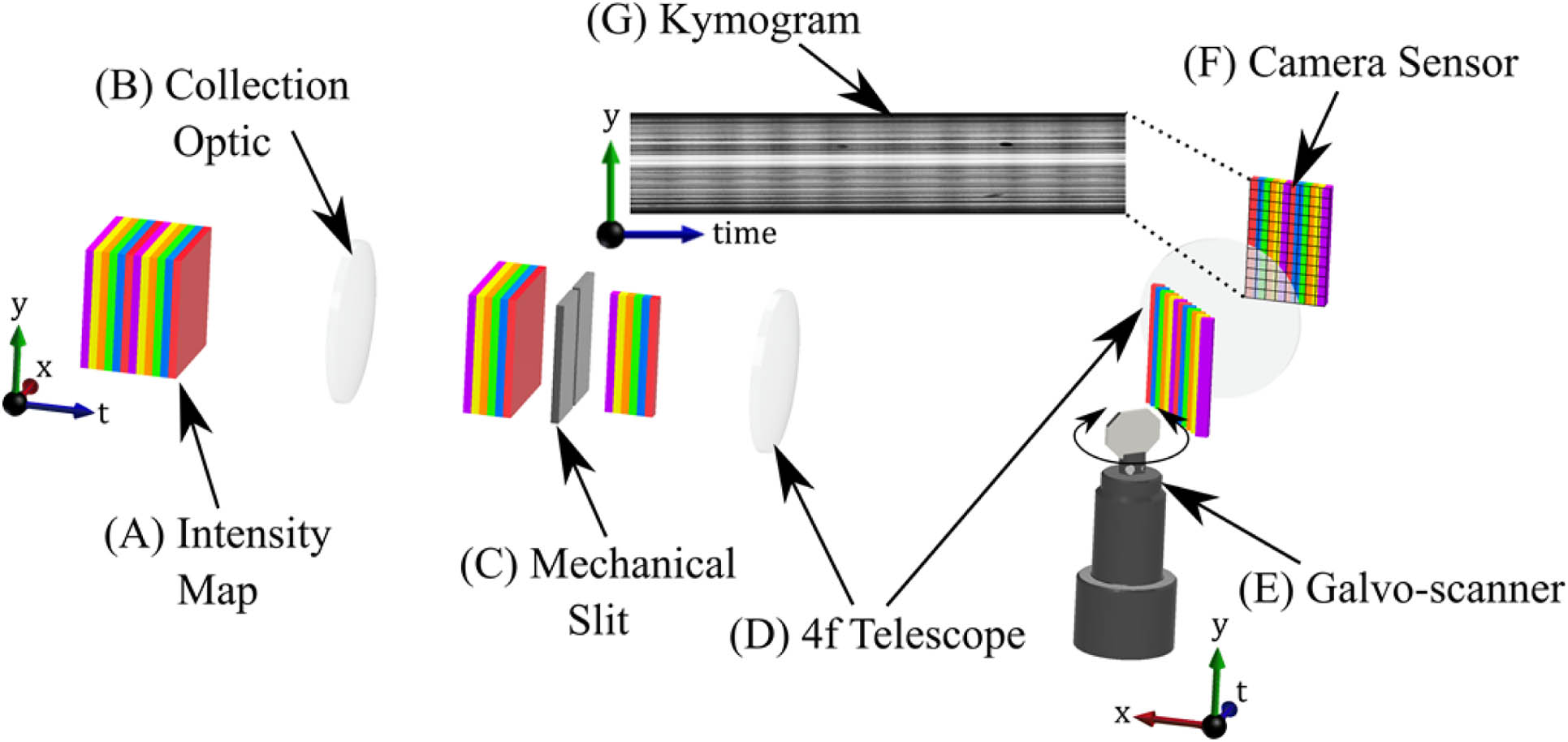
Figure 1.Intensity map (A) at the sample plane of a collection optic (B) is imaged to a narrow spatial mask (C) at the primary image plane. Individual colors indicate time steps. The mask constrains a single spatial dimension before the reduced intensity map is re-imaged to a detector by a 4f telescope (D). A galvo-scanner (E) at the telescope’s Fourier plane provides a constant velocity streaking operator, separating temporal information as a function of spatial position. The reduced and streaked scene is then imaged to the camera sensor (F) by the second
B. Optical System
An NV optical streaking magnetometer was designed around a laboratory-built widefield fluorescence microscope. A simplified CAD model of this system is provided in Fig. 2. Continuous optical excitation at 532 nm was provided by a frequency-doubled diode pumped solid-state
![]()
Figure 2.NV optical streaking magnetometer designed around a widefield fluorescence microscope is depicted. A 532 nm laser (green) was focused to the back focal plane of a long working distance objective (OBJ) by a plano–convex lens (L1). NV fluorescence (red) was separated from the source by a dichroic mirror (DM) and a long-pass filter LPF. The NV diamond sensor (NVD) was mounted on a printed circuit board with a co-planar microstrip RF antenna loop (RFA). An optical window at the center of the RF antenna allowed for illumination and fluorescence collection. A field coil (FC) was centered on the NV sensor such that spatially uniform magnetic fields could be generated. Spatially varying magnetic fields were generated with a permalloy electromagnetic needle (EM) wrapped with a coil fixed to a rotational mount. To reduce the amount of overlap between adjacent time steps, a mechanical slit (MS) was positioned at the primary image plane formed by the tube lens (L2). Optical streaking was achieved with a galvo-scanner (GS) positioned at the Fourier plane of a 4f telescope (L3 and L4) coupling the primary image plane to the detector (CMOS). Cylindrical beams and conic focal points are depicted to differentiate between infinity space and image planes, respectively. Components were not drawn to scale to assist with visibility of the optical path.
C. Magnetic Field Detection
Magnetic field detection was achieved by cw-ODMR [23,24]. A continuous
D. Hardware and Timing Control
Figure 3 shows the simplified hardware and connection diagram for the optical streaking system. System timing was synchronized by a rising edge delivered to an externally triggered digital pulse/delay generator (PGEN) (DG535, Stanford Research Systems) via a data acquisition (DAQ) card (National Instruments) controlled by custom LabVIEW software. The timing diagram in Fig. 3 shows the pulse control protocol for a single kymograph acquisition. Each waveform in the timing diagram is vertically offset and referenced to a common voltage
![]()
Figure 3.(Left) Simplified block diagram demonstrating the streak control system. A PC data acquisition card provided the TTL signal to start the PGEN and serial communications with the RF generator. System timing was provided by a digital PGEN through TTL signals sent to trigger the camera and a function generator. Magnetic field and ramp voltages were output from the function generator to the magnetic field coil and galvo-scanner, respectively. Continuous RF was amplified before being coupled to the NV diamond by a coplanar microstrip antenna loop. (Right) The optical streak system timing diagram is shown for a single acquisition period
E. Electromagnet Fabrication
Electromagnets were manufactured by acid etching 1 mm Permalloy 80 wire (KND1564, ESPI Metals) in an 8:7:5 ratio by volume solution of phosphoric acid, sulfuric acid, and DI water, respectively [25]. The Permalloy 80 consisted of 80% nickel, 5% molybdenum, and 15% iron. Stock solutions of 85% (wt/wt) phosphoric acid and 95% (wt/wt) sulfuric acid were mixed with DI water and transferred to a 10 mL glass vial. Etching was accomplished by electrolysis with the permalloy wire as the cathode and a filed steel nail as the anode. Sections cut from 200 μL Eppendorf pipette tips were used to protect permalloy surfaces not being etched as outlined in Ref. [25]. Voltage was applied, starting with 6 V DC for coarse etching, and reduced to 3 V DC once the exposed wire had visibly narrowed. The acid solution was reused to produce several needles; however, etching time was adjusted to account for increasing salt concentration. The coil was then wound with 44 American wire gauge (AWG) copper magnet wire until the coil was approximately 18 mm in length and had a resistance of
F. Minimum Detectable Field Analysis
The minimum detectable magnetic field sensitivity was evaluated by applying continuous illumination and RF coupling to the NV diamond. The sensor was centered both axially and radially on a large 9 cm diameter field coil designed to approximate uniform magnetic field intensity across the field of view. Streak images were acquired with a 225 ms exposure duration at 110 μm/ms (5 pix/ms) streak rate at the camera sensor verified with an optical chopper wheel. A mechanical slit at the primary image plane was adjusted to provide an image
In Eq. (1),
G. Optical Streaking NV Magnetometry
To demonstrate acquisition of both spatial and sub-millisecond temporal information within a single snapshot, an optically streaked sinusoidal magnetic field was measured from a spatially translating permalloy electromagnetic needle tip. The needle was fixed to a piezo-electric rotation mount such that the needle axis was orthogonal to the plane of the diamond. A serial trigger sent to the rotation mount translated the needle along the spatial axis of the NV diamond at a rate of
3. RESULTS AND DISCUSSION
A. Magnetic Field Optimization and Sensitivity Analysis
An optimization and magnetic sensitivity analysis was performed to demonstrate the NV sensor’s ability to detect sinusoidal magnetic field modulations during optical streaking [27]. A neodymium bias magnet was positioned near the sensor to ensure that the weak sinusoidal fields would overcome the 8–9 MHz of splitting exhibited by the NV sensor under zero-field conditions. A small amount of splitting in the
Streak images were obtained while scanning the RF from 2830 to 2910 MHz with a slit width of
![]()
Figure 4.Optimization and magnetic sensitivity analysis to demonstrate proper NV function as a magnetometer during optical streaking. (A) ODMR plot of the average intensity across each streak as a function of RF from 2830 to 2910 MHz acquired with an
Streak magnetic sensitivity was then optimized by performing a subsequent frequency sweep under an applied 40 Hz spatially uniform sinusoidal field. Profile plots of the normalized average intensity across each streak image were calculated (Fig. 4B) for each RF.
Figure 4C shows four RMS maxima that roughly coincide with the steepest tangent lines to the ODMR plot. The RMS amplitude of the intensity profiles at each RF was calculated using Eq. (1). It is to be expected that small changes in the Zeeman splitting bandwidth caused by magnetic field modulation would produce the maximum change in fluorescence intensity at these points. The vertical dashed red line at 2874 MHz indicates the RF with the best sensitivity to sinusoidal field oscillations. While it is possible, and quite common, to determine the optimal RF from the derivative of the ODMR curve in Fig. 4A, determining the optimal sensitivity from the RMS intensity provides validation for the optical streaking method [31].
The sinusoidal magnetic field profile in Fig. 4B and all field measurements that follow were acquired at 2874 MHz. A linear response was observed for magnetic field intensities down to approximately 10 μT (Fig. 4D), demonstrating an approximately linear trend in RMS intensity with respect to decreasing magnetic field strength over the observed range.
B. Optical Streaking NV Magnetometry
Our system was designed to capture sub-millisecond diffraction limited magnetic field variations of spatially propagating phenomena. As a validation, a chemically sharpened electro-magnetized permalloy needle tip was mechanically translated near the surface of the NV diamond during image acquisition.
Figure 5A shows a 50% transparent image of a standard 1951 USAF resolution test target registered with an image of the needle taken with a bright-field microscope immediately after streak acquisition. The needle tip was placed adjacent to the horizontal bars of group 3 element 3 with a known width of
![]()
Figure 5.Demonstration of magnetic field intensity plots obtained by optically streaking an electromagnetic needle moving laterally across the NV diamond sensor and validation of needle size. (A) A 50% transparent image of a 1951 USAF resolution test target was registered with an image of the needle such that the tip was adjacent to the horizontal bars of group 3 element 3 with a known width of 49.61 μm. (B) Magnetic field profile near the electromagnet imaged with the slit open and the needle stationary quantified by the change in fluorescence contrast from the background streak. A vertical dashed yellow line indicates the slice of the image captured by the narrow slit. The magnetic field intensity drops off sharply as the sharpened tip of the electromagnet recedes from the NV sensor that supports the
The magnetic field profile from the needle placed adjacent to the diamond (Fig. 5B) was acquired with the slit open, needle stationary, and 50 μT DC applied field. An image of the background intensity map without an applied field to the needle was subtracted to resolve the magnetic profile of the needle and the surrounding solenoidal field. Regions of positive contrast resulting from fields produced by the needle are found close to the needle tip, while negative contrast regions distant from the needle are due to the opposite orientation of the solenoidal field lines. The sharp drop-off in the magnetic field appears to correlate well with the
Background-subtracted lateral motion of the electromagnet at
A profile plot of the electromagnet path seen in Fig. 5D was created by plotting the intensities along a Manhattan trajectory represented by dashed horizontal yellow lines where the horizontal rows cross through the centroid of each bright region in Fig. 5C. A bandpass filter with 20 and 60 Hz corner frequencies was used with a sampling rate equal to the streak rate to reduce high-frequency noise components. The increase in fluorescence contrast resulting from the needle field is roughly 5%, while the solenoidal field has a negative 3% contrast. The total contrast falls within the
C. Future Direction and Applications
We have demonstrated optical streaking magnetometry with a maximum temporal resolution of
The maximum spatial extent for the optical arrangement in Fig. 2 is limited to 120 μm owing to the choice of optics and use of small (5 mm) two-axis galvo-scanner mirrors. Here the term spatial extent refers to the width of each streak to avoid confusion with the term field of view, usually reserved for spatial images. A single-axis large form factor mirror or a modification of the optical train could increase the spatial extent by a factor of up to 2.5 for the camera sensor that was used. System timing may need to be adjusted to account for changes in mirror inertia for larger galvo-mirrors [33]. While the current setup is limited to producing 2D kymograms, push broom raster scanning could be added to produce image stacks by translating either the mechanical slit or the sample for repeatable events [34].
While temporal resolution is governed primarily by the streak rate and slit width, both parameters are physically constrained by the available NV fluorescence emission. Using a sensor with a greater NV density would exhibit increased photon emission, allowing faster streak rates. It should be noted that faster streak rates would improve temporal resolution while decreasing the sequence duration. Compensation for shorter sequence duration could be made by adopting a large area sensor or wide aspect ratio sensor with the same pixel size but more pixels spanning the streak. The collection efficiency could also be increased with a higher-NA oil immersion objective, since the high refractive index of diamond results in modest losses at the NV–air boundary [35]. The magnetic field was acquired under continuous RF and optical stimulation without active or passive magnetic shielding, and no attempt was made to optimize RF antenna coupling to the NV.
This design has many potential applications where transient magnetic events can be isolated to a single spatial axis. Recent advances in NV sensors have resulted in sensitivities as low as
While NV magnetometry is a spin projection limited technique, sensitivity is heavily influenced by photon and technical noise sources, e.g., laser intensity, temperature, and mechanical vibrations. Pulse NV interrogation protocols, such as Hahn echo or dynamic decoupling, can be implemented for higher sensitivity for narrow bandwidth AC magnetic fields [2,37]. Such techniques can readily be combined with optical streaking systems to greatly improve magnetic sensitivity by introducing a static or time dependent field to average environmental interactions to zero [38]. Aside from dynamic decoupling, common mode rejection (CMR) strategies can also be used to differentially isolate signals from background fluorescence [20,39].
While this work focuses entirely on magnetic field imaging, optical streaking could potentially be applied to localization and monitoring of active biological processes such as ATPase activity [40], measurement of fast changing electric fields [41,42], dynamic relaxometry [43–45], and rapid pressure changes [46]. This technique could also be applied to a wide range of quantum sensors and applications beyond magnetic field imaging. Several other color centers exist including silicon vacancies [47], silicon carbide [48], optically addressable molecular spins [49], and upconversion particles [50,51].
This technique was primarily motivated by its capability to be readily extended to full 3D video acquisition by utilizing compressed sensing techniques with potential frame rates of 1.5 Mfps [52]. A translating magnetized needle tip was chosen because it is analogous to video of light pulse propagation seen in compressed ultrafast photography (CUP) [22]. By introducing a pseudo-random spatial mask in place of the mechanical slit, this system should be able to leverage numerical reconstruction techniques to produce single-shot magnetic field videos. Using knowledge of the optical streaking forward model and the addition of a random spatial mask, compressed 3D information can be recovered using inverse reconstruction algorithms [53,54].
NV diamonds also exhibit an all-optical longitudinal T1 relaxation that can detect the presence of paramagnetic species via the associated change in relaxation rate [43,44,55]. With sub-microsecond frame rates reported by Liu
4. CONCLUSION
We have demonstrated an optical streaking NV magnetometer capable of capturing magnetic fields with micro-scale spatial extent and
Acknowledgment
Acknowledgment. The authors thank Allen Kiester and Gary Noojin for their helpful advice and assistance with equipment. Thank you for all your support. Vladislav V. Yakovlev acknowledges the support from the NSF, AFOSR, DOD Army Medical Research, NIH, and CPRIT. Mark A. Keppler was supported by an NSF Graduate Research Fellowship. Work contributed by SAIC was performed under the United States Air Force. Joel N. Bixler received funding from AFOSR. Miloš Nesládek was funded by the Grant Agency of the Czech Republic.
References
[1] G. Davies, M. F. Hamer. Optical studies of the 1.945 eV vibronic band in diamond. Proc. R. Soc. London A, 348, 285-298(1976).
[2] J. F. Barry, J. M. Schloss, E. Bauch, M. J. Turner, C. A. Hart, L. M. Pham. Sensitivity optimization for NV-diamond magnetometry. Rev. Mod. Phys., 92, 015004(2020).
[3] S. Hernández-Gómez, N. Fabbri. Quantum control for nanoscale spectroscopy with diamond nitrogen-vacancy centers: a short review. Front. Phys., 8, 610868(2021).
[4] T. Zhang, G. Pramanik, K. Zhang, M. Gulka, L. Wang, J. Jing, F. Xu, Z. Li, Q. Wei, P. Cigler, Z. Chu. Toward quantitative bio-sensing with nitrogen–vacancy center in diamond. ACS Sens., 6, 2077-2107(2021).
[5] Y. Wu, F. Jelezko, M. B. Plenio, T. Weil. Diamond quantum devices in biology. Angew. Chem., 55, 6586-6598(2016).
[6] R. Schirhagl, K. Chang, M. Loretz, C. L. Degen. Nitrogen-vacancy centers in diamond: nanoscale sensors for physics and biology. Annu. Rev. Phys. Chem., 65, 83-105(2014).
[7] L. M. Pham, D. Le Sage, P. L. Stanwix, T. K. Yeung, D. Glenn, A. Trifonov, P. Cappellaro, P. R. Hemmer, M. D. Lukin, H. Park, A. Yacoby, R. L. Walsworth. Magnetic field imaging with nitrogen-vacancy ensembles. New J. Phys., 13, 045021(2011).
[8] J.-C. Jaskula, E. Bauch, S. Arroyo-Camejo, M. D. Lukin, S. W. Hell, A. S. Trifonov, R. L. Walsworth. Superresolution optical magnetic imaging and spectroscopy using individual electronic spins in diamond. Opt. Express, 25, 11048-11064(2017).
[9] J. M. Schloss, J. F. Barry, M. J. Turner, R. L. Walsworth. Simultaneous broadband vector magnetometry using solid-state spins. Phys. Rev. Appl., 10, 034044(2018).
[10] J. F. Barry, M. J. Turner, J. M. Schloss, D. R. Glenn, Y. Song, M. D. Lukin, H. Park, R. L. Walsworth. Optical magnetic detection of single-neuron action potentials using quantum defects in diamond. Proc. Natl. Acad. Sci. USA, 113, 14133-14138(2016).
[11] D. Le Sage, K. Arai, D. R. Glenn, S. J. Devience, L. M. Pham, L. Rahn-Lee, M. D. Lukin, A. Yacoby, A. Komeili, R. L. Walsworth. Optical magnetic imaging of living cells. Nature, 496, 486-489(2013).
[12] N. Mohan, C. S. Chen, H. H. Hsieh, Y. C. Wu, H. C. Chang.
[13] G. Kucsko, P. C. Maurer, N. Y. Yao, M. Kubo, H. J. Noh, P. K. Lo, H. Park, M. D. Lukin. Nanometre-scale thermometry in a living cell. Nature, 500, 54-58(2013).
[14] M. Fujiwara, S. Sun, A. Dohms, Y. Nishimura, K. Suto, Y. Takezawa, K. Oshimi, L. Zhao, N. Sadzak, Y. Umehara, Y. Teki, N. Komatsu, O. Benson, Y. Shikano, E. Kage-Nakadai. Real-time nanodiamond thermometry probing
[15] C. A. Hart, J. M. Schloss, M. J. Turner, P. J. Scheidegger, E. Bauch, R. L. Walsworth. N–V-diamond magnetic microscopy using a double quantum 4-Ramsey protocol. Phys. Rev. Appl., 15, 044020(2021).
[16] J. J. Davies. Optically-detected magnetic resonance and its applications. Contemp. Phys., 17, 275-294(1976).
[17] A. M. Wojciechowski, M. Karadas, A. Huck, C. Osterkamp, S. Jankuhn, J. Meijer, F. Jelezko, U. L. Andersen. Contributed review: camera-limits for wide-field magnetic resonance imaging with a nitrogen-vacancy spin sensor. Rev. Sci. Instrum., 89, 031501(2018).
[19] J. Malmivuo, R. Plonsey. Bioelectromagnetism Principles and Applications of Bioelectric and Biomagnetic Fields, 15(1995).
[20] J. L. Webb, L. Troise, N. W. Hansen, J. Achard, O. Brinza, R. Staacke, M. Kieschnick, J. Meijer, J. F. Perrier, K. Berg-Sørensen, A. Huck, U. L. Andersen. Optimization of a diamond nitrogen vacancy centre magnetometer for sensing of biological signals. Front. Phys., 8, 430(2020).
[21] K. Mizuno, H. Ishiwata, Y. Masuyama, T. Iwasaki, M. Hatano. Simultaneous wide-field imaging of phase and magnitude of AC magnetic signal using diamond quantum magnetometry. Sci. Rep., 10, 11611(2020).
[22] L. Gao, J. Liang, C. Li, L. V. Wang. Single-shot compressed ultrafast photography at one hundred billion frames per second. Nature, 516, 74-77(2014).
[23] V. M. Acosta, A. Jarmola, E. Bauch, D. Budker. Optical properties of the nitrogen-vacancy singlet levels in diamond. Phys. Rev. B, 82, 201202(2010).
[24] D. R. Glenn, R. R. Fu, P. Kehayias, D. Le Sage, E. A. Lima, B. P. Weiss, R. L. Walsworth. Micrometer-scale magnetic imaging of geological samples using a quantum diamond microscope. Geochem. Geophys. Geosyst., 18, 3254-3267(2017).
[25] B. D. Matthews, D. A. LaVan, D. R. Overby, J. Karavitis, D. E. Ingber. Electromagnetic needles with submicron pole tip radii for nanomanipulation of biomolecules and living cells. Appl. Phys. Lett., 85, 2968-2970(2004).
[26] . Magnetic field calculator for coil.
[27] A. Kuwahata, T. Kitaizumi, K. Saichi, T. Sato, R. Igarashi, T. Ohshima, Y. Masuyama, T. Iwasaki, M. Hatano, F. Jelezko, M. Kusakabe, T. Yatsui, M. Sekino. Magnetometer with nitrogen-vacancy center in a bulk diamond for detecting magnetic nanoparticles in biomedical applications. Sci. Rep., 10, 2483(2020).
[28] M. Mrózek, A. M. Wojciechowski, W. Gawlik. Characterization of strong NV—gradient in the e-beam irradiated diamond sample. Diam. Relat. Mater., 120, 108689(2021).
[29] R. Rubinas, V. V. Vorobyov, V. V. Soshenko, S. V. Bolshedvorskii, V. N. Sorokin, A. N. Smolyaninov, V. G. Vins, A. P. Yelisseyev, A. V. Akimov. Spin properties of NV centers in high-pressure, high-temperature grown diamond. J. Phys. Commun., 2, 115003(2018).
[30] T. Mittiga, S. Hsieh, C. Zu, B. Kobrin, F. Machado, P. Bhattacharyya, N. Z. Rui, A. Jarmola, S. Choi, D. Budker, N. Y. Yao. Imaging the local charge environment of nitrogen-vacancy centers in diamond. Phys. Rev. Lett., 121, 246402(2018).
[31] F. Alghannam, P. Hemmer. Engineering of shallow layers of nitrogen vacancy colour centres in diamond using plasma immersion ion implantation. Sci. Rep., 9, 5870(2019).
[32] Z. Ma, S. Zhang, Y. Fu, H. Yuan, Y. Shi, J. Gao, L. Qin, J. Tang, J. Liu, Y. Li. Magnetometry for precision measurement using frequency-modulation microwave combined efficient photon-collection technique on an ensemble of nitrogen-vacancy centers in diamond. Opt. Express, 26, 382-390(2018).
[33] M. Pothen, K. Winands, F. Klocke. Compensation of scanner based inertia for laser structuring processes. J. Laser Appl., 29, 012017(2017).
[34] S. Ortega, R. Guerra, M. DIaz, H. Fabelo, S. Lopez, G. M. Callico, R. Sarmiento. Hyperspectral push-broom microscope development and characterization. IEEE Access, 7, 122473(2019).
[35] D. A. Hopper, H. J. Shulevitz, L. C. Bassett. Spin readout techniques of the nitrogen-vacancy center in diamond. Micromachines, 9, 437(2018).
[36] M. Parashar, K. Saha, S. Bandyopadhyay. Axon hillock currents enable single-neuron-resolved 3D reconstruction using diamond nitrogen-vacancy magnetometry. Commun. Phys., 3, 174(2020).
[37] D. Suter, F. Jelezko. Single-spin magnetic resonance in the nitrogen-vacancy center of diamond. Prog. Nucl. Magn. Reson. Spectrosc., 98–99, 50-62(2017).
[38] D. Suter, G. A. Álvarez. Colloquium: protecting quantum information against environmental noise. Rev. Mod. Phys., 88, 041001(2016).
[39] M. Mrózek, D. Rudnicki, P. Kehayias, A. Jarmola, D. Budker, W. Gawlik. Longitudinal spin relaxation in nitrogen-vacancy ensembles in diamond. EPJ Quantum Technol., 2, 22(2015).
[40] L. P. McGuinness, Y. Yan, A. Stacey, D. A. Simpson, L. T. Hall, D. Maclaurin, S. Prawer, P. Mulvaney, J. Wrachtrup, F. Caruso, R. E. Scholten, L. C. L. Hollenberg. Quantum measurement and orientation tracking of fluorescent nanodiamonds inside living cells. Nat. Nanotechnol., 6, 358-363(2011).
[41] M. Block, B. Kobrin, A. Jarmola, S. Hsieh, C. Zu, N. L. Figueroa, V. M. Acosta, J. Minguzzi, J. R. Maze, D. Budker, N. Y. Yao. Optically enhanced electric field sensing using nitrogen-vacancy ensembles. Phys. Rev. Appl., 16, 024024(2021).
[42] F. Dolde, H. Fedder, M. W. Doherty, T. Nöbauer, F. Rempp, G. Balasubramanian, T. Wolf, F. Reinhard, L. C. L. Hollenberg, F. Jelezko, J. Wrachtrup. Electric-field sensing using single diamond spins. Nat. Phys., 7, 459-463(2011).
[43] F. Gorrini, R. Giri, C. E. Avalos, S. Tambalo, S. Mannucci, L. Basso, N. Bazzanella, C. Dorigoni, M. Cazzanelli, P. Marzola, A. Miotello, A. Bifone. Fast and sensitive detection of paramagnetic species using coupled charge and spin dynamics in strongly fluorescent nanodiamonds. ACS Appl. Mater. Interfaces, 11, 24412-24422(2019).
[44] S. Steinert, F. Ziem, L. T. Hall, A. Zappe, M. Schweikert, N. Götz, A. Aird, G. Balasubramanian, L. Hollenberg, J. Wrachtrup. Magnetic spin imaging under ambient conditions with sub-cellular resolution. Nat. Commun., 4, 1607(2013).
[45] F. Perona Martínez, A. C. Nusantara, M. Chipaux, S. K. Padamati, R. Schirhagl. Nanodiamond relaxometry-based detection of free-radical species when produced in chemical reactions in biologically relevant conditions. ACS Sens., 5, 3862-3869(2020).
[46] M. W. Doherty, V. V. Struzhkin, D. A. Simpson, L. P. McGuinness, Y. Meng, A. Stacey, T. J. Karle, R. J. Hemley, N. B. Manson, L. C. L. Hollenberg, S. Prawer. Electronic properties and metrology applications of the diamond NV-center under pressure. Phys. Rev. Lett., 112, 047601(2014).
[47] S. Lagomarsino, A. M. Flatae, H. Kambalathmana, F. Sledz, L. Hunold, N. Soltani, P. Reuschel, S. Sciortino, N. Gelli, M. Massi, C. Czelusniak, L. Giuntini, M. Agio. Creation of silicon-vacancy color centers in diamond by ion implantation. Front. Phys., 8, 626(2021).
[48] S. Castelletto, A. Boretti. Silicon carbide color centers for quantum applications. J. Phys. Photon., 2, 022001(2020).
[49] S. L. Bayliss, D. W. Laorenza, P. J. Mintun, B. D. Kovos, D. E. Freedman, D. D. Awschalom. Optically addressable molecular spins for quantum information processing. Science, 370, 1309-1312(2020).
[50] F. Vetrone, R. Naccache, A. Zamarrón, A. J. De La Fuente, F. Sanz-Rodríguez, L. M. Maestro, E. M. Rodriguez, D. Jaque, J. G. Sole, J. A. Capobianco. Temperature sensing using fluorescent nanothermometers. ACS Nano, 4, 3254-3258(2010).
[51] X. Liu, A. Skripka, Y. Lai, C. Jiang, J. Liu, F. Vetrone, J. Liang. Fast wide-field upconversion luminescence lifetime thermometry enabled by single-shot compressed ultrahigh-speed imaging. Nat. Commun., 12, 6401(2021).
[52] X. Liu, J. Liu, C. Jiang, F. Vetrone, J. Liang. Single-shot compressed optical-streaking ultra-high-speed photography. Opt. Lett., 44, 1387-1390(2019).
[53] E. J. Candès, J. Romberg, T. Tao. Robust uncertainty principles: exact signal reconstruction from highly incomplete frequency information. IEEE Trans. Inf. Theory, 52, 489-509(2006).
[54] S. Voronin, C. Zaroli. Survey of computational methods for inverse problems. Recent Trends in Computational Science and Engineering, 3(2018).
[55] V. Radu, J. C. Price, S. J. Levett, K. K. Narayanasamy, T. D. Bateman-Price, P. B. Wilson, M. L. Mather. Dynamic quantum sensing of paramagnetic species using nitrogen-vacancy centers in diamond. ACS Sens., 5, 703-710(2020).


Set citation alerts for the article
Please enter your email address

© Copyright 2018-2021 | Chinese Laser Press. All Rights Reserved 沪ICP备15018463号-20